
At present, due to the rising storage density of Flash Memory storage devices and the continuous upgrading of chip production process nodes, processes within 20 nanometers are becoming more and more common in the manufacture of memory devices. The radiographic examination also brings new challenges. The experiment proves that under the long-term X-ray irradiation of the memory chip, due to the electronic transition, it will bring about the loss of data, which will invalidate the product system. X-ray inspection is an indispensable means of reliability during the assembly process. In order to avoid damage to the chip, we propose the following solutions for your reference to help factory engineers reasonably avoid product failure when using X-ray equipment.
1. Flash memory absorption X-ray ability test
1. Test process:
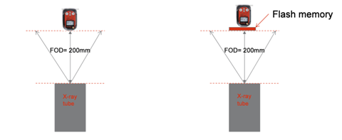
- •KV=100KV, focus to chip distance=200mm
- • Set different target power and record the X-ray intensity without chip
- • Set different target power and record the X-ray intensity after placing the chip
- • Calculate the X-ray intensity difference, this value is the X-ray energy absorbed by the chip
2. Test results:
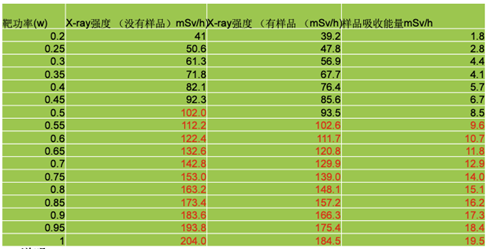
Description: Due to range limitation, RADEYE G-10 (max100mSv/h), the red part of the value is the calculated value
Flash memory X-ray absorption test
in conclusion:
KV=100KV, FOD=200mmX-ray (mSv/h) energy absorbed by the chip = 18+ 22 * (Target Power – 0.2W)
3. According to the user's daily testing parameters, define the maximum allowable testing time
Select the normal detection setting conditions:- • KV: 100KV
- • Target power 0.5 W
- • Sample to focus distance (FOD): 27.5mm
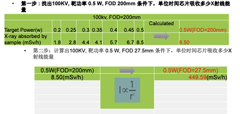
Detection time (seconds) = 3.75 / 449.59 * 3600 = 30 Sec
Maximum X-ray exposure time of the sample ≤ 30 sec. The sample absorbs X-ray energy less than 0.375 Rad, and the inspection process is safe.
Second, how to prevent damage to the memory chip during X-ray inspection
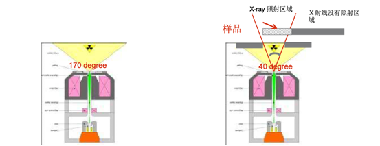
1. Add collimator
Reduce the XX ray cone angle from 170 degrees to about 40 degrees.Purpose: To detect one of the chips, the other chips will not be irradiated (memory chips are usually arranged centrally).
As shown below
2. Fully automatic chip detection using FNC program
Fixed detection parameters using FNC:KV: 100KV
Target power: 0.5W
Distance between focus and sample: 27.5mm
Automatically complete the detection, and the total exposure time of the chip is controlled by the machine