Please submit your message online, we will contact you as soon as possible!

Author:A
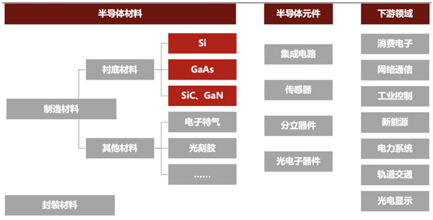
In the entire semiconductor industry chain, semiconductor materials are in the upstream, the middle reaches are all kinds of semiconductor components, and the downstream applications include consumer electronics, communications, new energy, power, transportation and other industries. In recent years, with the second and third generation compound semiconductors achieving wider applications with their unique physical properties, their upstream substrate materials gallium arsenide, silicon carbide and gallium nitride have attracted more and more attention in China. This research report will focus on these three types of substrate materials.
Compound semiconductor refers to the semiconductor material formed by two or more elements, which can be divided into binary compounds, ternary compounds, quaternary compounds, etc., according to the number of elements, and binary compound semiconductors can also be divided into III-V group, IV-IV group, II-VI group, etc., according to the position of the constituent elements in the periodic table of chemical elements. At present, compound semiconductor materials represented by gallium arsenide (GaAs), gallium nitride (GaN) and silicon carbide (SiC) have become the fastest developing, most widely used and largest output semiconductor materials after silicon.
The field of semiconductor substrate materials has undergone three stages of development:
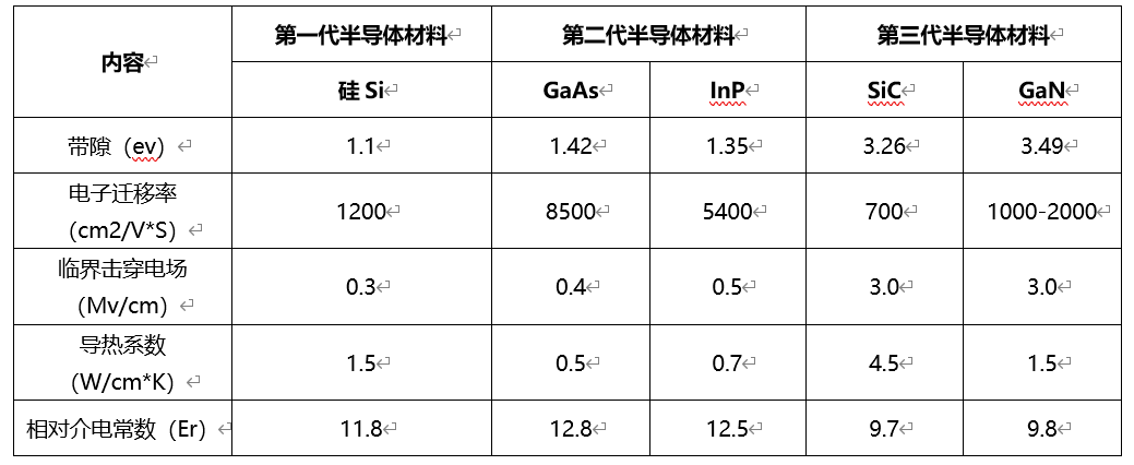
The first stage is the 1950s, silicon Si as the representative of the first generation of semiconductor materials made of diodes and transistors replaced the electron tube, mainly used in low-voltage, low-frequency, low-power transistors and detectors, such as computer CPU, GPU, memory, mobile phone SoC and other devices, led to the integrated circuit as the core of the microelectronics industry rapid development. However, the physical properties of silicon material limit its application in optoelectronics and high-frequency electronic devices, such as its indirect band gap characteristics determine that it can not obtain high electro-optical conversion efficiency, and its band gap width is narrow (1.12 eV), saturated electron mobility is low (1450 cm2/V·s), which is not conducive to the development of high-frequency and high-power electronic devices.
The second stage is the beginning of the 1990s, with the development of the semiconductor industry, the physical bottleneck of silicon materials has become increasingly prominent, the second-generation semiconductor materials represented by gallium arsenide GaAs and indium phosphide InP have emerged, and the preparation technology of related devices has gradually matured, making semiconductor materials enter the field of optoelectronics. GaAs good optical performance makes it widely used in optical devices, but also in the need of high-speed devices in special occasions, is the 4G era of most of the communication equipment materials, such as millimeter wave devices, light emitting devices, satellite communications, mobile communications, optical communications, GPS navigation and so on. However, the band gap (which reflects the strength of valence electrons being bound, directly determines the voltage resistance and maximum operating temperature of the device) is not large enough, and the breakdown electric field is low, which limits its application in the field of high temperature, high frequency and high power devices, and arsenic is toxic.
The third stage is the third generation semiconductor materials represented by silicon carbide SiC and gallium nitride GaN in recent years, which have significant advantages in key parameters such as band gap width, breakdown electric field strength, saturated electron drift rate, thermal conductivity and radiation resistance, further meeting the needs of modern industry for high power, high voltage and high frequency, and being the main materials in the 5G era. For high temperature, high frequency, anti-radiation, high-power devices; Blue, green, violet diode, semiconductor laser, etc.
At present, more than 95% of the world's chips and devices are based on silicon as the substrate material, due to the great cost advantage of silicon materials, the future in all kinds of discrete devices and integrated circuits in the field of silicon will still occupy a dominant position, but the unique physical characteristics of compound semiconductor materials, giving it unique performance advantages in RF, optoelectronics, power devices and other fields.
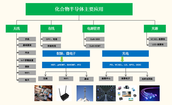
Photo source: SEMI, Sinolink Securities Research Institute
According to the different resistance, gallium arsenide materials can be divided into semiconductor type and semi-insulating type. Due to its high resistivity and high frequency performance, semi-insulated gallium arsenide substrate can make MESFET, HEMT and HBT structure circuits, mainly used in radar, satellite television broadcasting, microwave and millimeter wave communication, wireless communication (represented by mobile phones) and optical fiber communication, mainly used to make PA components in mobile phones. It has 85% market share in the high frequency power amplifier market. Semiconductor gallium arsenide single crystals account for about 60% of the total GaAs market and are mainly used in optoelectronic devices such as leds and VCsels (vertical resonator surface-emitting lasers).
Gallium arsenide single crystal wafer production process can be divided into:
1, polycrystalline cleaning: gallium arsenide polycrystalline into the mixture of ammonia, hydrogen peroxide and pure water configuration, cleaning in the cleaning tank with water; Wash with ultrasonic flat oscillator, remove surface impurities, and then dehydrate with methanol; PBN crucible cleaning process is the same as polycrystalline cleaning process.
2. Single crystal growth: the cleaned gallium arsenide polycrystals are put into the PBN crucible, the crucible is put into the quartz tube and vacuum the quartz tube with a vacuum pump. After sealing, the quartz cotton (thermal insulation) is wrapped outside into the single crystal furnace, so that the crystal can complete growth in the single crystal furnace and grow into a single crystal rod.
3. Demoulding: After the end of single crystal growth, the single crystal furnace is cooled, and the quartz tube is cut with an open tube saw after being lowered to room temperature, and the PBN crucible is separated from the gallium arsenide crystal, and the gallium arsenide crystal is removed.
4. Crystal processing: the tail cover of the removed gallium arsenide crystal rod is cut off with a band saw, the outer circle is ground by an external grinder, the test sample is taken with an internal circular saw, and the crystal is judged according to the test sample.
5. Crystal slicing: Gallium arsenide crystal rods are cut into wafers of a certain thickness on a multi-line cutting machine, and water-based solution and cutting powder are used to cool down during cutting. After cutting, rinse the chip, soak in alcohol and air dry.
6, wafer grinding: the surface of the wafer in the cleaning tank is pre-cleaned with ammonia, hydrogen peroxide and pure water mixture to clean the impurities on the surface of the wafer to make the surface cleaner; Then the grinding machine chip is used to grind, remove the damaged layer of the chip, and ensure the consistency of thickness.
7. Wafer polishing: The polished wafer is put into the polishing machine, wet polishing under the action of polishing liquid, so that the surface reaches a fine mirror, and then the surface is cleaned with ammonia, hydrogen peroxide and pure water mixture in the cleaning tank, and then the dryer is dehydrated and dried.
8. Wafer cleaning: Clean the wafer with a mixture of ammonia, hydrogen peroxide and pure water to remove the dust and chemical residues remaining on the surface of the wafer after processing in the previous process, and package the dried wafer as a finished product after passing the inspection.
Since the 1950s, a variety of gallium arsenide single crystal growth methods have been developed. At present, the mainstream industrial growth processes include: liquid-sealed Czochra method (LEC), horizontal Bridgman method (HB), vertical Bridgman method (VB) and vertical gradient solidification method (VGF).
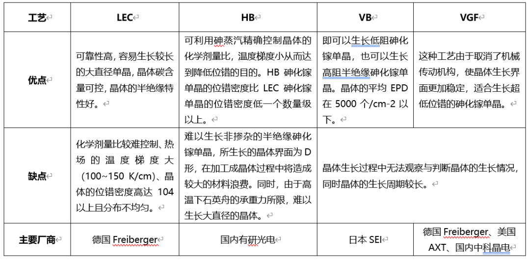
Compound semiconductor because the overall scale of the industry is small, the degree of non-standardization is high, and the contract manufacturing model is mainly. Europe and the United States dominate the gallium arsenide industry chain, and Taiwan manufacturers monopolize foundry. Sumitomo of Japan, Freiberger of Germany and AXT of the United States together account for about 90% of the global market share of semi-insulated substrates. Limited by the size of the substrate, the current production line is mainly 4 inch and 6 inch wafers, and some companies have also begun to introduce 8 inch production lines, but it has not yet formed the mainstream. Because gallium arsenide is mainly an Emitterbase-Collector vertical structure, the number of transistors is only on the order of 100. The silicon wafer is the plane design of the Source Gate Drain, and the number of transistors reaches tens of millions of orders of magnitude, so gallium arsenide does not have obvious advantages in process research and development as the silicon wafer foundry industry.
Sumitomo is the world's highest level of semi-insulated gallium arsenide monocrystals. It mainly produces gallium arsenide by VB method and can mass produce 4 inch and 6 inch monocrystals. Germany Freiberger mainly uses VGF, LEC method to produce 2 to 6 inches gallium arsenide substrate, all products are used in the field of microelectronics; Half of the AXT products in the United States are used for leds and half are used as microelectronic substrates. Domestic suppliers of gallium arsenide substrate is mainly used in LED chips, a few companies such as Yunnan Germanium industry for radio frequency gallium arsenide substrate gradually released.
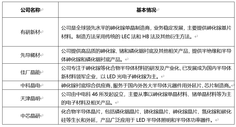
Domestic manufacturer
SiC material as a substrate has achieved large-scale application, through epitaxial growth, device manufacturing and other links, can be made into silicon carbide based power devices and microwave radio frequency devices, in the silicon carbide chip cost structure 60%-70% is the substrate and epitaxial sheet, of which the substrate accounts for about 40%-50%, is the third generation of semiconductor industry development of important basic materials.
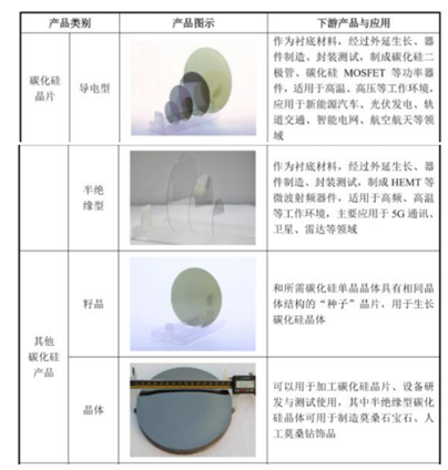
As a semiconductor substrate material, silicon carbide wafer can be divided into conductive type and semi-insulating type according to different resistivity. Among them, conductive silicon carbide wafers are mainly used in the manufacture of high temperature and high voltage resistant power devices, which are widely used in new energy vehicles, photovoltaic power generation, rail transit, smart grid, aerospace and other fields, and the market is large. Semi-insulated silicon carbide substrate is mainly used in microwave radio frequency devices and other fields, such as 5G communication, radar, etc., with the acceleration of 5G communication network construction, the market demand is more obvious.
The main preparation process of SiC substrate is roughly divided into two steps: the first step is SiC powder (high purity silicon powder and high purity carbon powder) in the single crystal furnace after high temperature sublimation to form SiC ingot in the single crystal furnace; The second step is to roughing, cutting, grinding and polishing the SiC ingot to obtain a transparent or translucent SiC wafer with no damaged layer and low roughness (that is, SiC substrate).
(1) Raw material synthesis. High purity silicon powder and high purity carbon powder were mixed according to a certain ratio, and silicon carbide particles were synthesized at high temperature above 2,000℃. After crushing, cleaning and other processes, the high purity silicon carbide powder raw materials which meet the requirements of crystal growth are prepared.
(2) Crystal growth. The silicon carbide crystals were grown by physical vapor transfer (PVT) or high temperature chemical vapor deposition (HTCVD) in a crystal growth furnace with high purity silicon carbide powder as raw material. For example, the PVT method places the high-purity silicon carbide powder and seed crystal respectively in the lower and top of the cylindrical closed graphite crucible in the single crystal growth furnace, heating the crucible to more than 2,000℃ through electromagnetic induction, controlling the temperature at the seed crystal slightly lower than the lower powder, forming an axial temperature gradient in the crucible. The sic micropowder sublimes to form vapor phase Si2C, SiC2, Si and other substances at high temperature, and reaches the seed crystal at lower temperature driven by temperature gradient, and crystallizes on it to form cylindrical sic ingot.
(3) ingot processing. The obtained silicon carbide crystal ingot was orientated by X-ray single crystal orientator, then ground and rolled, and processed into standard diameter silicon carbide crystal.
(4) Crystal cutting. Using multi-line cutting equipment, silicon carbide crystals are cut into thin sheets with a thickness of no more than 1mm.
(5) Wafer grinding. The wafer is ground to the desired flatness and roughness by diamond grinding fluids of different particle sizes.
(6) Chip polishing. The polished silicon carbide without surface damage was obtained by mechanical polishing and chemical mechanical polishing.
(7) Chip detection. Use optical microscope, X-ray diffractometer, atomic force microscope, non-contact resistivity tester, surface flatness tester, surface defect comprehensive tester and other instruments and equipment to detect the microtubule density, crystal quality, surface roughness, resistivity, warpage, curvature, thickness change, surface scratch and other parameters of silicon carbide wafer. According to this, the quality level of the chip is determined.
(8) Chip cleaning. The silicon carbide polishing sheet is cleaned with cleaning agent and pure water to remove the residual polishing liquid and other surface dirt on the polishing sheet, and then the wafer is blown and shaken dry by ultra-high purity nitrogen and drying machine; The wafer is encapsulated in a clean sheet box in a super-clean chamber to form a downstream ready-to-use silicon carbide wafer.
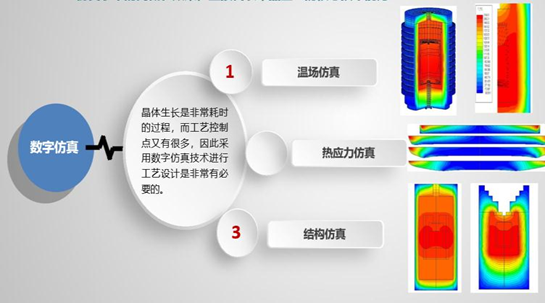
Photo source: Sinolink Securities Research Institute
Single crystal growth temperature is 2350-2500 degrees, because the temperature in the furnace can not be measured, through high-precision digital simulation technology can save a lot of research and development time and cost, the level of simulation also directly represents the core technical capabilities of single crystal enterprises.
3. Single crystal growth technology
The slow growth of single crystal is an important reason for the high cost of SIC substrate. At present, both Cree and domestic mainstream manufacturers use PVT physical vapor transfer method. Because the growth rate of silicon carbide crystals is much slower than that of silicon crystals, 8-inch silicon wafers can grow to 1-2 meters in 2-3 days, while 4-inch silicon carbide wafers can only grow 2-6cm a week. An important factor affecting crystal growth is seed crystal propagation, which is the "seed" wafer with the same crystal structure as silicon carbide single crystal, and is the source of crystal growth. Seed crystal growth is the core technology of silicon carbide preparation, and it is also one of the core technologies to judge all silicon carbide substrate enterprises, and seed crystals are generally not sold.
Silicon carbide single crystal growth technology
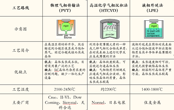
Photo source: Sinolink Securities Research Institute
4. Single crystal processing technology
Because the hardness of silicon carbide is very high and the brittleness is high, the grinding, cutting and polishing are time-consuming and the yield is low. Silicon cutting takes only a few hours, while 6-inch silicon carbide cutting takes hundreds of hours.
Silicon carbide processing
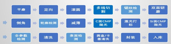
Photo source: Sinolink Securities Research Institute
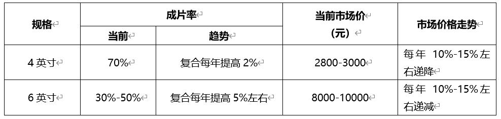
(4) Domestic substrate prices and trends
At present, the 4-inch silicon carbide substrate in the market is relatively mature, the yield is higher, and the price is lower, while the 6-inch substrate price is much higher than the 4-inch sheet due to the small supply and low sheet yield. The three major driving forces to reduce the cost of SIC substrate in the future are: process and equipment improvement to speed up crystal growth; Defect control improvement to improve yield; Design improvements reduce the substrate area of the used device.
Domestic silicon carbide substrate price and trend
5. Global competition pattern
At present, the SiC chip market is mainly dominated by the United States, Europe and Japan, and Chinese enterprises are beginning to emerge. According to Yole's forecast, the compound annual growth rate of SiC will reach 31% from 2017 to 2023, reaching a market size of about $1.5 billion in 2023. According to the "China's third-generation semiconductor Silicon Carbide Chip Industry Analysis Report 2020" data from the Semiconductor Times Industry Data Center, in the global semiconductor SiC chip market in the first half of 2020, the United States CREE shipments accounted for 45% of the world; European companies are strong in the field of design and development of SiC devices, the main companies are Siltronic, ST, IQE, Infineon, etc. Japan has strong technical force and complete industrial chain. The representative enterprises are Panasonic, Rohm, Sumitomo Electric, Mitsubishi, etc. SiCrystal, a subsidiary of Rohm, accounts for 20% and II-VI accounts for 13%. Chinese enterprises are developing rapidly, with Tianke Heda's market share rising from 3% in 2019 to 5.3% in 2020, and Shandong Tianyue accounting for 2.6%.
Global semiconductor SiC wafer market share in the first half of 2020
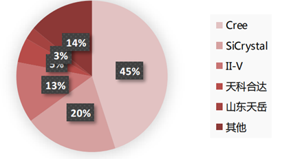
Source: Semiconductor Age Industry Data Center
Gallium nitride (GaN) - third generation semiconductor material
Limited by technology and process level, GaN material as a substrate to achieve large-scale application is still facing challenges, because gallium nitride material itself has a high melting point, and requires high pressure environment, it is difficult to use melting crystallization technology to make GaN substrate. At present, GaN substrates made of gallium nitride thick film are mainly grown on Al2O3 sapphire substrate, and then the substrate and gallium nitride thick film are separated by stripping technology, and the separated gallium nitride thick film can be used as the epitaxial substrate. The previous mainstream of this substrate was 2 inch caliber, and now there are 4 to 6 inch substrates. The advantage is that the dislocation density is significantly low, but the price is expensive, thus limiting the application of gallium nitride thick film substrates.
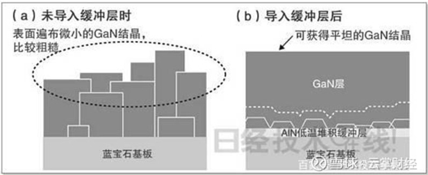
At present, the commonly used ammonia phase method (or HVPE method) requires a growth temperature of more than 1000℃, so single crystal sapphire (Al2O3) has attracted attention as a substrate whose characteristics are still stable under high temperature ammonia. Due to the large difference in the chemical properties (chemical bonding), thermal expansion coefficient and lattice constant of GaN and sapphire, the surface of GaN crystals grown on sapphire is as rough as frosted glass, and the crystal defects are very many, and it is impossible to obtain high-quality GaN that can be used in semiconductor components. In 1986, Isamu Akasaki, a professor at Nagoya University's Faculty of Engineering, developed the low-temperature buffer layer technology. The technology uses aluminum nitride (AlN) as a buffer layer for stacking, and GaN crystals with few crystal defects and flat surface can be grown on the sapphire substrate.
GaN substrate production technology
Due to the high hardness of GaN materials, high melting point characteristics, high substrate production difficulty, low yield, slow technological progress, the cost of GaN wafers is still high, in 2005, the 2-inch GaN substrate cost of $20,000, the price is still at the level of $3,000, in contrast, the 4-inch GaAs substrate cost only 100-200 yuan. At present, GaN can be grown on SiC, Si, sapphire, diamond and other substrates by epitaxy technology, which can effectively solve the problem of the limitation of GaN substrate materials.
From the perspective of the global GaN substrate market pattern, Japanese manufacturers occupy a leading position in GaN substrates, including Sumitomo Electric, Mitsubishi Chemical, Sumitomo Chemical, etc., and the three Japanese companies have a combined market share of more than 85%. Domestic enterprises engaged in GaN single crystal growth, mainly Suzhou Nawei, Dongguan Gallium, Shanghai Gallium special and core Yuan-based.
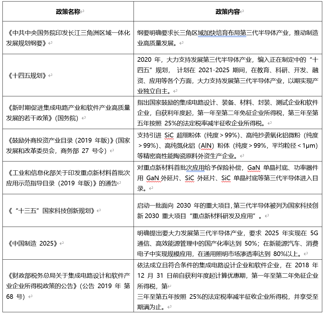
5. Policy support for compound semiconductors
Disclaimer | This article is the author's original, reproduced only for industry sharing and exchange, does not represent the views of the department, copyright belongs to the original author. In case of infringement, please contact us. In addition, if you reprint this article, please indicate the source.
If you are interested in this article, please immediatelycontact us

Support Hotline
Please submit your message online, we will contact you as soon as possible!