Please submit your message online, we will contact you as soon as possible!

Author:Bingfeng big country heavy high-end electronic components
Gallium arsenide is a better material than silicon, electrons move through gallium arsenide five times faster than silicon, and gallium arsenide is less sensitive to ambient temperature than silicon. But microchips and solar cells are made of silicon, and because silicon is an abundant element, it costs less to make electronics and photovoltaic products from silicon than gallium arsenide. Now, researchers at the Massachusetts Institute of Technology (MIT) have found a way to replicate solar cell or microchip designs onto gallium arsenide using graphene, and that could all change.
Sang-Hoon Bae, a postdoctoral researcher in MIT's Department of Mechanical Engineering, said: "We can apply this technique to materials such as gallium arsenide or gallium nitride, and we are working on solar cells. Gallium arsenide is a good candidate material for solar cells. In our approach, we can copy and paste gallium arsenide freestanding films, so we can expect to reduce manufacturing costs."
As researchers at the Massachusetts Institute of Technology in the United States begin to study photovoltaic devices using a lower-cost graphene production process, faster flexible electronics and more efficient solar cells become the application prospects of gallium arsenide.
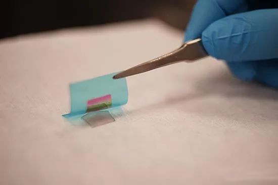
MIT researchers have devised a way to grow single-crystal compound semiconductors through two-dimensional materials on their substrates. The compound semiconductor film is then stripped through a flexible substrate, showing a rainbow of colors from the film interference. Photo credit: MIT/Wei Kong and Kuan Qiao
The replicative production process involves a gallium arsenide wafer and a layer of graphene on top of it. Gallium and arsenide are poured onto graphene covered with gallium arsenide wafers, and then gallium and arsenide atoms are arranged to form a copy of the underlying gallium arsenide wafers, which can be tens to hundreds of nanometers thick, and can finally be stripped off the graphene to produce a thin film replica of the wafers. This technique is known as "remote epitaxy".
This technology allows the rapid production of gallium arsenide films using a single wafer, greatly reducing manufacturing costs. "Not only can gallium arsenide and gallium nitride be made, it's a general method and we can make other materials," Bae added. Lithium fluoride is another material that is being tested for this manufacturing process. Because the process can produce thin films, it could be used to build suitable multifunctional devices, such as flexible solar cells, which the Bae team is working on, or wearable sensors. Researchers have even proposed mobile phones attached to the skin.
The researchers think the process is like two magnets interacting through a piece of paper, with gallium having a negative charge and arsenic having a positive charge, and this difference means that their atoms interact through graphene and are subsequently arranged in parallel copies to form a gallium arsenide crystal structure.
Bae's team collaborated with researchers from Sun Yat-sen University in China, the University of Virginia, the University of Texas at Dallas, the Naval Research Laboratory, Ohio State University, and Georgia Institute of Technology. The study was supported in part by the U.S. Defense Advanced Research Projects Agency, the U.S. Department of Energy, the U.S. Air Force Research Laboratory, LG Electronics of Korea, AmorePacific Group of Korea, Collin Research Corporation of the United States, and Analog Devices of the United States.
| Some of the materials are from high-end electronic components. They are reproduced only for industry sharing and exchange and do not represent the views of our company. The copyright is reserved by the original author. In case of infringement, please contact us. In addition, if you reprint this article, please indicate the source.
If you are interested in this article, please immediatelycontact us

Support Hotline
Please submit your message online, we will contact you as soon as possible!