Abstract: A novel single wafer cleaning technique has been developed to meet the needs of compound semiconductor manufacturing: removing photoresist and post-etching residues while maintaining compatibility with various compound semiconductor materials, exposed metals, and dielectric layers. The CoatsClean platform is a combination of process and chemical technologies that significantly reduce chemical use, shorten process time, wafer to wafer consistency, and process flexibility. This paper describes the CoatsClean technique and demonstrates the ability to remove post-etching residues in the production of polyimide through hole and base layer GaAs heterojunction bipolar transistors (HBT).
coats Cleaning process description
The CoatsCleanTM process uses a newly developed EVG-301RS monolithic photoresist stripping system specifically designed to implement the CoatsCleanTM technology. Remove with a stripper formulated with organic solvent. The CoatsCleanTM process is a multi-step process executed in a bowl that keeps the tool footprint small. Wafer-coated, formulated strippers have enough volume to completely cover the top surface of the wafers, with significantly less chemical use per wafer compared to immersion or single wafer spray tools. Next, the formula is heated on the chip using point heating. Using point heating provides the flexibility to process in different wafer types in the same tool and in the same bowl. After heating, first rinse the formula with a small amount of fresh formula, then rinse with water spray.
Finally, the wafer is dried by rotary drying. In addition to reducing the use of chemicals, the use of fresh, unused solutions on each chip results in chip-to-chip consistency and increases the stability of the chemical formula because the chemicals stored in the tool are kept at room temperature rather than at higher cleaning temperatures. Overall, the CoatsCleanTM technology offers a new method of photoresist removal and wafer cleaning that offers environmental sustainability and a lower cost of ownership compared to traditional photoresist strip processes.
Polyimide VIA resist strip
The coated CleanTM technology was used to remove the post-etching residue from two different etching processes. The first process is the polyimide obtained by etching between metal-1 and metal-2. The holes are formed in a positive photoresist and then etched by polyimide using o2 plasma. The remaining photoresist is removed from the polyimide below and a single 150mm wafer is coated with a coating cleaning formula. After 30 seconds of exposure to the coating cleaning formula dissolving, the wafer is rinsed with fresh formula, then rinsed with deionized water spray, and then dried by rotary drying. The total process time for one wafer is less than 2 minutes, and the total volume usage per wafer formulation is less than 40mL.
Figure 1 shows SEM images of the CoatsCleanTM resist strip before and after the process, clearly showing the removal of the resist layer in the underlying polyimide film. The blades are inspected using the Rudolph NSX-100 automatic optical inspection system. Figure 2 shows a wafer diagram from NSX that shows the die yield of the coated transparent film stripped wafer, indicating good stripping performance. Electrical characteristics are required to ensure device performance on wafers machined using photovoltaic strips.
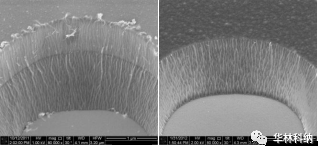
图1 光伏剥离工艺的扫描电镜图像:[左]未剥离,显示光致抗蚀剂(顶层)和聚酰亚胺(底层),涂覆后[右]剥离,仅显示聚酰亚胺层
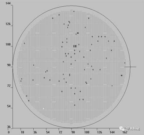
Figure 2 NSX-100 PV strip process wafer diagram showing 99.3% chip yield
Figure 3 shows SEM images before and after the CoatsCleanTM banding process, clearly showing the removal of residue after etching on the BP platform. CoatsCleanTMBP strip process was used to remove the BP etched residue on four full-flow wafers. These wafers are inspected using the Rudolph NSX-100 automatic optical inspection system. The wax map from NSX compared to wafers stripped using the standard Sky Factory process (solvent-based bath and spray cleaning), as shown in Figure 4, shows comparable stripping performance. Electrical characterization is required to ensure device performance of chips treated with CoatsCleanTM.
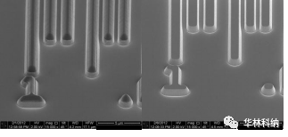
FIG. 3 SEM image of BP stripping process :[left] without stripping and [right] after coating stripping
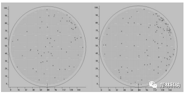
Figure 4 NSX-100 wafer diagram of BP bar on full-flow wafer :[left] CoatsCleanTM wafer yield of 99.4%, [right] standard Skyworks wafer yield of 99.1%
conclusion
We have developed a new single chip cleaning technology that meets the manufacturing needs of gallium arsenide HBT. The CoatsCleanTM technology successfully removed the photoresist after the PV etching process and removed the etched residue after the BP etching process. Photovoltaic strip and BP strip have short process time and low chemical usage. (Article Number: HLKN-21-1129-3)
Disclaimer | Part of the material is from Warincona, reproduced only as an industry sharing exchange, does not represent the views of the company, copyright belongs to the original author. In case of infringement, please contact us. In addition, if you reprint this article, please indicate the source.
If you are interested in this article, please immediatelycontact us