Please submit your message online, we will contact you as soon as possible!

Author:国盛证券
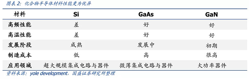
Semiconductor materials can be divided into two categories of elemental semiconductor and compound semiconductor, the former such as silicon (Si), germanium (Ge) and other semiconductors, the latter for gallium arsenide (GaAs), gallium nitride (GaN), silicon carbide (SiC) and other compounds formed. In the past, the semiconductor has mainly experienced three generations of changes, gallium arsenide (GaAs), gallium nitride (GaN) and silicon carbide (SiC) semiconductors as representatives of the second and third generation semiconductors, compared with the first generation of semiconductor high-frequency performance, high temperature performance is much better, the manufacturing cost is more expensive, can be described as the upstart in semiconductors.
Beyond Moore: Optical, RF, power and other analog ics continue to evolve
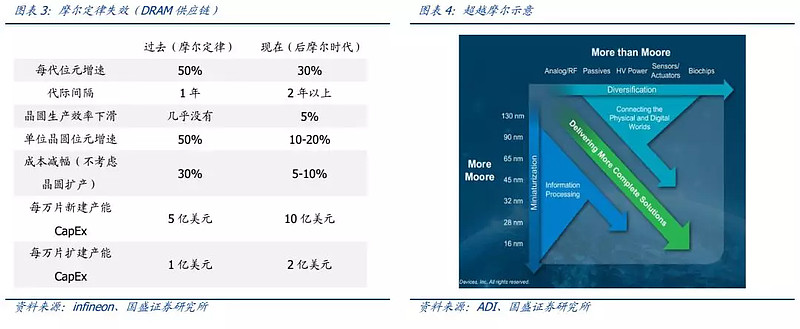
Moore's Law slowed down, and integrated circuits diverged. There are two main reversals in the development of integrated circuits: More Moore (depth of moles) and More than Moore (beyond moles). Moore's Law states that in about 18 months of integrated circuits, the number of transistors in the same area will double, but the price will drop by half. However, the 28nm encountered obstacles, although the number of transistors doubled, but the price did not drop by half. "More Moore" refers to continuing to improve the process node technology and entering the post-Moore period. At the same time, More than Moore was proposed, which was more application-oriented and focused on adding more and more functionality to a single chip IC.
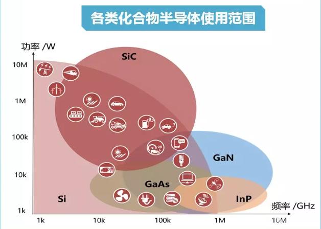
Third generation semiconductors adapt to more application scenarios. Silicon-based semiconductor has the advantages of high temperature resistance, good radiation resistance, convenient manufacture and good stability. High reliability features, so that more than 99% of integrated circuits are made of silicon. However, silicon-based semiconductors are not suitable for use in high-frequency, high-power fields. The main material of PA in the era of 2G, 3G and 4G is GaAs, but after entering the 5G era, the main material is GaN. 5G has a higher frequency, and its jumping reflection characteristics make it a shorter transmission distance. Because millimeter wave has very high requirements for power, and GaN has the characteristics of small volume and large power, it is currently the most suitable PA material for the 5G era. Third generation semiconductors such as SiC and GaN will be more adaptable to future application needs.
Analog IC focuses on voltage and current control, distortion rate, power consumption, reliability and stability, and designers need to consider the impact of various components on the performance of analog circuits, which is difficult to design. Digital circuits pursue computing speed and cost, mostly using CMOS technology, which has been developing along Moore's Law for many years, constantly using more efficient algorithms to process digital signals, or using new processes to improve integration and reduce costs. The excessively high process node technology is often not conducive to the realization of analog ics to achieve low distortion and high signal-to-noise ratio or output high voltage or high current to drive other components, so analog ics have a relatively low demand for node evolution than digital ics. The life cycle of analog chips is also long, generally up to 10 years or more, such as Fairchild's operational amplifier μA741 launched in 1968, which has been sold for nearly 50 years and is still used by customers.
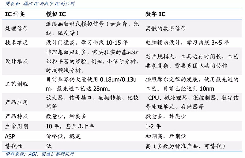
At present, digital ics mostly use CMOS processes, while analog ics use more types of processes and are not bound by Moore's Law. Analog IC manufacturing processes include Bipolar process, CMOS process and BiCMOS process. In the high-frequency field, SiGe, GaAs and SOI processes can also be combined with Bipolar and BiCMOS processes to achieve even better performance. In the field of power, the SOI process and BCD (integrated DMOS and other power devices on the basis of BiCMOS) process also have better performance. Analog ics are widely used, and their use is also different, so the manufacturing process will also change accordingly.
Gallium arsenide (GaAs) : the core material for wireless communications, benefiting from the 5G megateny
Compared with the first generation of silicon semiconductors, gallium arsenide has the characteristics of high frequency, radiation resistance and high temperature resistance, so it is widely used in mainstream commercial wireless communications, optical communications and national defense and military applications. The popularity of wireless communication and the limitation of silicon on high frequency characteristics have led to the emergence of gallium arsenide materials, which have been widely used in the field of wireless communication.
Baseband and RF modules are the core components to complete 3/4/5G cellular communication functions. An RF module is generally composed of a transceiver and a front-end module (PA, Switch, Filter). Gallium arsenide has become the mainstream material for PA and Switch.
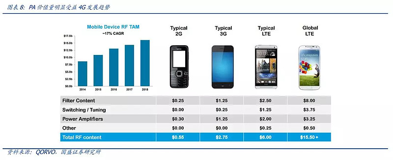
4G/5G frequency bands continue to increase, driving PA usage growth. Since a single PA chip can only process signals in a fixed frequency band, the increase in the cellular communication frequency band will significantly increase the PA consumption of a single smartphone. With the popularity of 4G communications, the frequency band of mobile communications has rapidly expanded from 6 in 2010 to 43, and the 5G era is expected to increase to more than 60. At present, the mainstream 4G communication uses 5 frequency 13 mode, the average use of 7 PA, 4 RF switches.
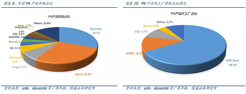
At present, gallium arsenide leading enterprises are still dominated by IDM mode, including Skyworks, Qorvo, Broadcom/Avago, Cree, Infineon and so on. At the same time, we also noticed that the industry development model began to gradually shift from IDM model to design + foundry production, typical events are the continued increase in the proportion of foundry, avago last year sold Colorado plant to Wen Mo and so on. We believe that GaAs substrate and device technologies continue to mature and standardize, product diversification, the value of device design is significant, and the design + manufacturing division pattern is beginning to increase.
According to estimates from third-party research institutions such as Yole Development, the global GaAs device market for PA reached $8-9 billion in 2017, and most of the market share was concentrated in Skyworks, Qorvo, and Avago. It is expected to officially exceed $10 billion in the next two years with the upgrade of communications.
If you are interested in this article, please immediatelycontact us

Support Hotline
Please submit your message online, we will contact you as soon as possible!