Please submit your message online, we will contact you as soon as possible!

Author:知乎:石大小生
Wafer-level packaging (WLP) is the packaging process in which most of the process is operated on the wafer (large wafer), the demand for wafer-level packaging (WLP) is not only subject to the requirements of smaller package size and height, but also must meet the requirements of simplifying the supply chain and reducing the overall cost, and improving the overall performance.
Wafer-level packaging provides a great advantage of flip chip technology, flip chip chip face down to the printed circuit board (PCB), can achieve the shortest electrical path, which also guarantees higher speed, reducing cost is another driving force for wafer-level packaging.
The device is packaged in batch, and the entire wafer can be packaged all at once. The cost of packaging a device on a given chip does not change with the number of bare chips per chip because all processes are steps of addition and subtraction using the mask process.
There are two types of WLP technology:
In general, there are two types of WLP technology: "fan-in" and "fan-out" wafer-level packages.
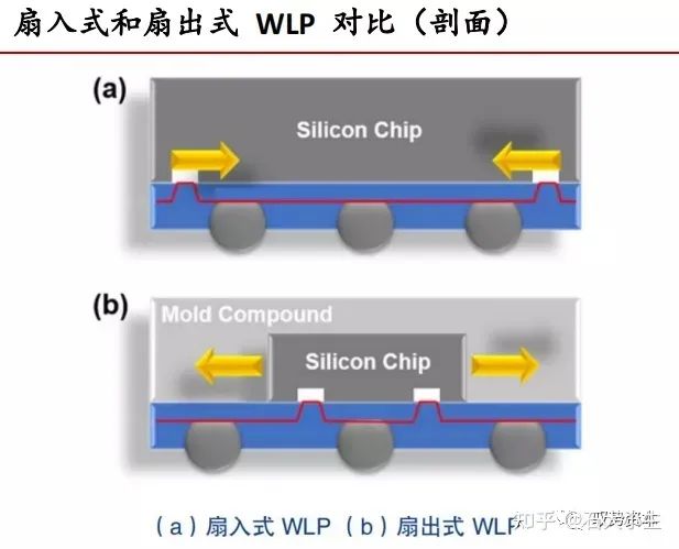
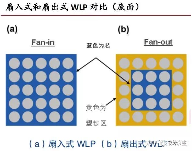
Traditional fan-in WLP is formed when the wafer is not cut. On the bare chip, the two-dimensional plane size of the final packaged device is the same as the size of the chip itself. After the device is fully packaged, the device can be singulated.
Thus, fan-in WLP is a unique form of packaging with the remarkable characteristics of true bare chip size. WLP with fan-in design is typically used in processes with low input/output (I/O) numbers (typically less than 400) and small bare metal sizes.
On the other hand, with the development of packaging technology, fan-out WLP has gradually appeared. Fan-out WLP is initially used to reassemble or reconfigure individual bare pieces into a wafer process and, based on this, form a final package through batch processing, construction, and metallization of structures such as traditional fan-in WLP back-end processing.
Fan-out WLP can be divided into chip First (Die First) and chip Last (Die last) according to the process, chip first on the process, simply put the chip on first, and then do wiring (RDL), chip on is to do wiring first, test the qualified unit and then put the chip on. The advantage of the chip back-on process is that it can improve the utilization rate of qualified chips to improve the yield, but the process is relatively complex.
eWLB is a typical chip-first Fan out process, and the chip-first process is adopted by JTRC Star Jinpeng FAN-OUT and Amkor's Portuguese factory. TSMC's INFO is also a chip-first Fan-out product. Anrely and ASE also have their own mature on-chip Fan-out processes.
In the history of the development of electronic equipment, the promotion of WLP packaging technology has produced many new products.
For example, thanks to the use of WLP, MOTOROLA was able to launch its RAZR phone, which was also its thinnest phone at launch. The latest model of the iPhone uses more than 50 WLP, and smartphones are the biggest driver of WLP development.
As the price of gold wire rises, some companies are also considering WLP as a low-cost alternative to lead-bonded packaging, especially for devices with higher pin counts. In recent years, WLP has also been widely used in image sensor applications. Currently, through-silicon (TSV) technology has been incorporated into WLP solutions for packaging image sensors. Other newer packaging technologies are also being developed and integrated with existing WLP technologies, such as three-dimensional (3D) integration.
If you are interested in this article, please immediatelycontact us

Support Hotline
Please submit your message online, we will contact you as soon as possible!