Please submit your message online, we will contact you as soon as possible!

Author:KANA
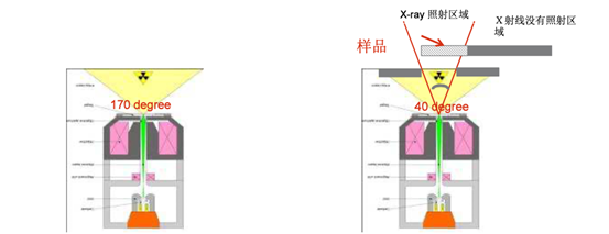
At present, due to the rising storage density of Flash Memory storage devices and the continuous updating of chip production process nodes, the process within 20 nm is becoming more and more common in the manufacturing of memory devices. The continuous expansion of line width not only brings challenges to manufacturing, but also brings new challenges to the X-ray inspection during the assembly process. The experiment proves that the memory chip will lose the data due to the electronic transition under the X-ray irradiation for a long time, so that the product system will fail. X-ray inspection is an indispensable reliability means in the assembly process, in order to avoid damage to the chip, we propose the following solutions for your reference to help factory engineers in the use of X-ray equipment reasonably avoid product failure.
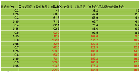
Note: Due to range limitation, RADEYE G-10 (max100mSv/h), the value in red is the calculated value
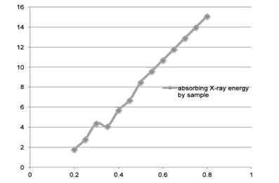
Flash memory 吸收X射线能力测试X-ray absorption capability test of Flash memory
Conclusion:
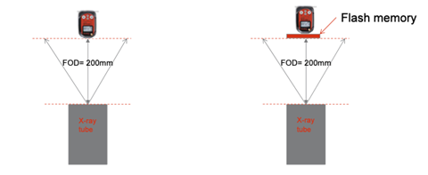
KV=100KV, FOD=200mm
X-ray (mSv/h) energy absorbed by the chip = 18+ 22 * (Target Power - 0.2W)
3. Define the maximum allowable detection time based on daily detection parameters
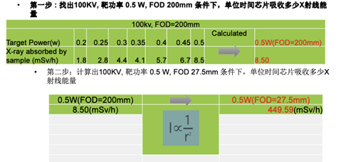
Select the usual detection setting condition:
• KV:100KV
• Target power 0.5W
• Sample to focus distance (FOD): 27.5mm
4. Problem: In the actual sound field process, it is difficult to control the X-ray inspection time within 30 seconds, in addition, to achieve standardized batch operation, it is also different from the usual operation.
If you are interested in this article, please immediatelycontact us

Support Hotline
Please submit your message online, we will contact you as soon as possible!