Please submit your message online, we will contact you as soon as possible!

Author:Bin Wang, Kana Technology
System-in-Package (SIP) and
Embedded Component Package (ECP) for 5G Systems
BinWang, Kana Technology
Mar.2020
5G has brought telecommunication technology to theupsurge and it has become the center of many hot topics since 2018, suchas IoT, AR/VR, Cloud, Big data, AI, Smart city and smart life, andautonomous vehicles … Fast data transfer and low latency are the two keyadvantages of 5G technology. This makes
5G the basis for the above technologies.The implementation of 5G will generate a huge demand for advanced packagingsolutions, since these solutions can be tailored to have the rightperformance features. There are many types of advanced packagingsolutions, such as SIP, heterogeneous integration, FOWLP and ECP. As aleader of electronics assembly and semiconductor assembly equipmentsolution provider, K&S has solutions covering almost all advanced packagingsolutions, while SIP and ECP are the two focus points. Kana technology isthe agent for K&S in these solutions. In general, 5G phones wouldcontain 10%-20% more SIPs than 4G phones. And ECP packages is expected toprosper in the era of 5G for the sake of its main advantages in shortsignal route, fast head dissipation and thin packages.
Figure 1: SIP Modules in 5G Phone
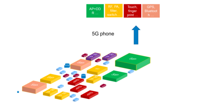
There are many different definitions forSIP. One of the best might be: a fully functional subsystem contains one ormultiple IC dies (bare or packaged 2D/3D), passive components, and possiblyIPDs (integrated passive devices), ECs (embedded components), and performanceenhancements (such as head dissipation lids, shielding, and stiffeners...). SIP is flexible in design and supply chain management,therefore fast timeto market. Traditional SIP adopts wire bonding, while advanced SIP adopts flipchip (FC) technology. ECs normally are categorized separately from SIPalthough it is might be part of SIP.Usually one advanced SIP unit contains 3 to5 FC dies. As the advent of 5G technology, more and more features need tobe integrated into one SIP unit. SIP for 5G would contain more FC dies,generally more than 10, or even 30 in one single unit. The firstconsideration in the assembly process is how to place so many FC dies athigh speed but still at competitive cost. Traditional FC bonders can handleonly one type of FC die. It is a nightmare to connect many FC bonders in aproduction line to handle 30 FC dies. In addition, the quantity of FC diesvaries between different models. It is not a feasible way to move FC bondersfrom line to line to suit different FC quantities in different SIP models. WithK&S Hybrid placement system, passive components (mainly 01005) and FCdies can be placed consequentially in one machine and one pass, regardlessthe quantity of FC dies. To do this, die sorting of FC dies from waferto tape and reel package is required. 15-25 microns can be achieved for FCdies placed in this way. This is also the accuracy level required byalmost all current substrate-based SIP applications. Moreover, the placementcost of FC dies is almost the same as that of passive components. Amongmany SIP types, RF modules are pushing the assembly process capabilities to thelimit. Economic spec. for materials and machines is not a key topicanymore. What more important is to make things
done.
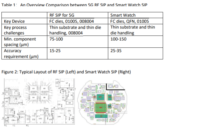
Th above comparison tells us that astandard SIP unit is very similar to a common SMT product. The technical requirements are very close to standard SMT. However, an advanced SIPproduct (typically RF SIP) requires much more. The component spacing is falling beyond normal SMTprocess requirements, which requires higher placement accuracy, as well as higher first pass yield toavoid impractical rework for such high dense assemblies. Next main consideration in the assembly process of advanced SIP is the handlingof thin substrates. Thin substrate with warpage is very common in semi-conductor back end assemblyprocesses. But people who are from standard SMT plants would very probably neglect this becausestandard SMT do not use vacuum support. Vast experience and data prove that a well-designed vacuumsupport would greatly improve the placement accuracy and yield, especially for veryhigh-component-density advanced SIP units. Ensuring a good thin substrate handling is the step to return the wholeprocess to a normal state. For standard SIP products, a vacuum support is not so critical. 008004 mass assembly is another challenge. It has been observed in advanced SIPproducts that more than 80% passive components were 01005 from 5 years before. 01005 mass assemblyis a mature process now, but 008004 is not yet. With 5G, 008004 will be widely used inadvanced SIP products. Many equipment vendors claimed their 008004 capability in specification. Butonly one or two succeed in real applications. Accuracy is the necessity but not the only factor for thesuccess of 008004 placement. Special attention should be paid to the stencil design and printingprocess, as well as low force control. The component is as thin as, and as fragile as FC dies. Onlyplacement force control triggered Z-stop placement process can adapt to the requirement effectively. Inaddition, a robust contact detection between 008004 and substrate is quite important. It isdifficult to have a real time contact detection under high speed placement process. There is a unique featureof Hybrid system that uses vacuum leakage detection principle to interpret a real time contact. Thebasic rule is that a separate vacuum loop will be destroyed once there is a contact between thecomponents and the substrate. Under this special technology, component cracks are controlled atminimum.
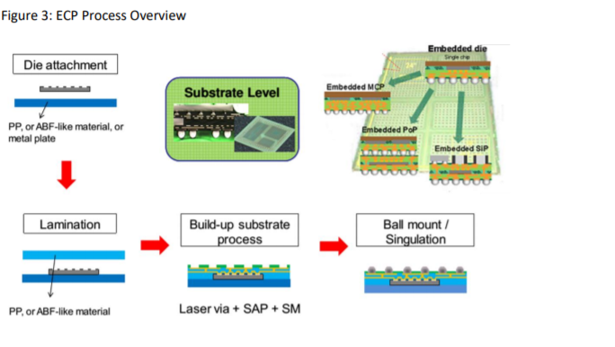
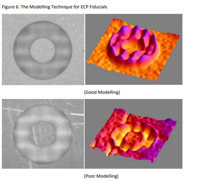
Embedded component packages (ECP) embed active dies and/or passive components into the base structure of a package or a substrate/PCB. They are categorized into 4 segments depending on the difference of base material: embedded component in laminate (substrate), embedded component in PCB (printed circuit board), embedded component in FPC (flexible printed circuit), and embedded interconnections in substrate. Without any printing or soldering process, ECP process need to be integrated into a substrate/PCB/FPC manufacturing process. As a result, the main players of ECP are PCB manufacturers. Typically, components (dies or passives) are firstly placed into cavities of a copper layer with PP or ABF-like tape in the back, then followed by a lamination process. Next are substrate/PCB building-up processes such as laser via, SAP, SM … In an ECP package, components are well protected in the base material, therefore yielding a very reliable interconnection. ECP also has the advantages of low profile (embedded), and short signal route, which fits the requirements of 5G applications quite well. Due to the special processes involved in the multi-layer PCB manufacturing, ECP normally requires a very high placement accuracy for both active dies (<10 µm @ 3 σ), and passive components (<20 µm @ 3 σ). It was known in the market that Hybrid system has proven its performance in a few tier 1 PCB manufacturers. Accuracy specification of many platforms uses a small panel and place components in a small region. But ECP applications use very large panels (around 610mmx546mm) to achieve a good cost structure. Placement in large panels yields much lower accuracy. As a result, the larger the test panel size and placement test region, the higher the actual accuracy in final applications. Hybrid system uses a test panel that has the size close to ECP applications.
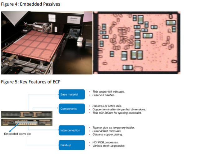
Bare dies in ECP applications have unique features. They are not solder bumps or copper pillars. The terminations are flat at the bottom, with very irregular patterns. As a result, it also demands a special algorithm to align them. In addition, the dies are thin, in most cases 50-200µm. The handling and placement of such thin dies is one of the top challenges in ECP processes. Force control no more than 0.5N is required. Under special circumstance, even 0.3N might be required. In a Hybrid placement system, thin dies are handed with the same method that is applied for 008004, which has been discussed in the above paragraph. Besides placement process, die ejecting and pickup process is also critical. Ejector pins need to be designed as multiple contact points, and a gentle Z-moving profile is necessary. Gentle pickup of dies is also mandatory. Hybrid systems calculated the pickup height dynamically, thus make it possible for a gentle pickup. With a Hybrid system for ECP application, the risk of die cracks is reduced to minimum. Reference: 1. Yole Development, 2017 and 2018 report 2. K&S Internal Estimate Jan 2019 3. Prismark/Binghamton University Report 4. “All in one Package” The Packaging Solution of the Future? AT&S (SIP China 2017)
If you are interested in this article, please immediatelycontact us

Support Hotline
Please submit your message online, we will contact you as soon as possible!