Abstract: By improving the fixture of inductively coupled plasma (ICP) equipment, the heat conduction efficiency of back helium was improved, the temperature difference between the bottom electrode base and the wafer surface was reduced, and the cooling effect was improved. The effects of RF power, ICP power, bottom electrode base temperature, chamber pressure and other parameters on the etching rate, selection ratio, inclination Angle and side wall smoothness of the through-hole on the back of SiC were analyzed. Through the improvement of fixture and the optimization of process conditions, the SiC through hole conditions were developed with the etching rate of 1μm/min, the selection ratio of SiC to Ni greater than 60∶1, the inclination Angle less than 85° and smooth side wall. It can be used for backside through hole etching of SiC GaN high electron mobility transistor (HEMT), SiC metal semiconductor field effect tube (MESFET) and other high power microwave devices and microwave monolithic integrated circuit (MMIC) development and production, and can shorten the process time and reduce the production cost.
Key words: silicon carbide; Back through hole etching; Inductively coupled plasma (ICP); Etching rate; Selection ratio
Introduction
SiC and GaN are the typical representatives of the third generation of semiconductor materials after Si and GaAs. The semiconductor microwave power devices and their microwave monolithic integrated circuits (MMIC) produced by them have the advantages of high operating temperature, high application frequency, large power output and high gain [1-2]. Due to the high thermal conductivity and stability of SiC material and its good lattice matching with GaN material, epitaxial GaN material on SiC substrate has become the main direction of GaN power device development, especially in the field of high-performance GaN high electron mobility transistor (HEMT) microwave power device and its MMIC. At present, epitaxial GaN material on SiC substrate is basically used [3]. In order to reduce the parasitic inductance at the source end of the device, GaN and SiC microwave power devices need to be grounded through holes to improve the frequency characteristics of the devices as much as possible [4]. Whether it is SIC-based GaNHEMT and its MMIC, or SiC metal semiconductor field effect tube (MESFET) and its MMIC, the main etching material on the back of the through hole process is SiC material, and the through hole etching process on the back of SIC-based chip has become one of the key processes to improve the frequency characteristics and reliability of the device. And SiC material has stable chemical properties and high bonding energy, there is no public reporting of mature wet etching technology, dry etching methods mainly include reactive ion etching (RIE reactiveionetching), electron cyclotron resonance (electroncyclontronresonance, ECR) etching, inductivelycoupledplasma (ICP) etching, due to ICP etching has higher plasma density, higher plasma energy, better cooling structure and plasma density and energy can be independently controlled advantages, ICP has the advantages of faster etching rate, better uniformity and consistency than other methods. There are three main problems in etching SiC in the past: first, the etching rate is low, which can not meet the increasing demand for production capacity; Second, although the etching rate can be improved by increasing the RF power, the selectivity can not meet the production demand. Third, increasing the electrode base temperature can also increase the etching rate, but the etching polymer will increase. When the polymer increases to a certain extent, a layer of micro mask will be formed at the bottom of the etching rate, resulting in a decline in the etching rate. By optimizing gas composition and gas pressure, Zhou Rui et al. [5] obtained the through hole etching rate of SiC up to 0.7μm/min, and the selective etching ratio of SiC to Ni was 60∶1. A. Borker et al. [6] reported that the etching rate was 1.3μm/min and the selective etching ratio of SiC to Ni was 35∶1 by means of ring-coupled RF output and multistage magnetic enhanced plasma density.
Increasing plasma density or energy in various ways to improve the etching rate is one of the main methods commonly used in the etching process. However, whether increasing plasma density or energy, the surface temperature of the wafer will increase during the etching process. As the surface temperature of the wafer increases, the above-mentioned etching polymer problem will become prominent. Therefore, cooling in the process of etching has always been a hot topic in the research of etching technology. International and domestic research on this cooling mainly focuses on reducing the limit temperature of the lower electrode (even as low as -100℃) by using new coolant and new cooling methods (such as liquid nitrogen, etc.), and then reducing the temperature of the wafer surface, but the effect of reducing the wafer surface temperature is not ideal [7]. The ICP device used in this paper is cooled by cooling liquid, the lower limit temperature of coolant is 0℃, and helium gas is passed between the lower electrode and wafer to improve the cooling effect. In this study, the ICP chip loading fixture is improved to improve the cooling effect. Through the improvement of fixture and the optimization of process conditions, the ideal SiC through hole process conditions were realized, which showed that the etching rate and selection ratio were increased simultaneously, the sidewall polymer was significantly reduced and the etching inclination Angle was lower than 85°. 1 Experimental design
1.1Sample preparation
A rectangular sample with an etching pattern of 25μm×50μm was prepared by sputtering base metal, photoetching pattern and electroplating thickened metal mask (mask Ni thickness is 3μm) on the 4H-SiC high purity semi-insulating substrate material, and the sample was cut into 1cm×1cm rectangular sample by grinding wheel scribing machine for use. Before each etching, it is glued to a sapphire substrate with a thickness of 3mm and a diameter of 3 inches (1 inch =2.54cm). In order to reduce the influence of the sapphire substrate on the etching results and make the experimental process as close as possible to the actual process, a Ni mask with a thickness of 3μm is electroplated on the sapphire substrate through the above process. 1.2Experimental process
SF6 gas was mainly used in the etching SiC experiment. In order to study the influence of the improved fixture on the etching results, a comparative experiment was conducted using two fixtures, and the influence of different electrode base temperature, different chamber pressure, different RF power, different ICP power and other process parameters on the etching results was analyzed. (The temperature variation range was set at ±0.5℃. The variation range of chamber pressure, RF power and ICP power is set at ±1%, and the variation range of RF reflected power and ICP reflected power is within ±2% of the positive power set value). During the process, the wafer surface temperature is directly measured by the variable temperature test paper, and the base temperature of the lower electrode is controlled by the temperature control equipment (the temperature variation range is set at ±0.5℃). In this experiment, other process parameters were fixed on the basis of the basic process conditions (temperature 10℃, chamber pressure 1.33Pa, RF power 150W, ICP power 1500W). The influence of single process parameters on etching rate (ratio of etching depth to total etching time), selection ratio (ratio of etching rate of SiC to etching rate of mask Ni), slope Angle and sidewall smoothness was obtained. 1.3 Result Characterization Scanning electron microscopy (SEM) was used to observe the polymer residue on the surface of the sample after etching, the inclination Angle after etching, and the smoothness of the side wall. The depth of etching was measured by a step meter. 2Results and discussion
Figure 1 shows the comparison before and after the improvement of the structure of the fixture. The biggest difference of the improved fixture is that a sealing ring is added between the metal pressing block and the wafer.
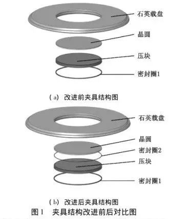
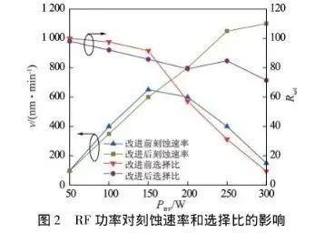
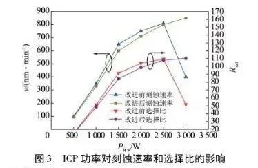
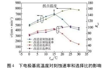
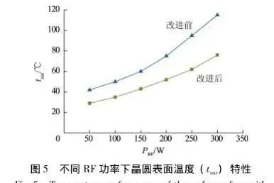
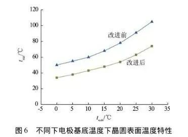
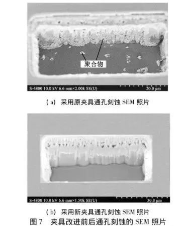
FIG. 2, FIG. 3 and FIG. 4 show the influence curves of RF power (PRF), ICP power (PICP) and lower electrode base temperature (tsub)(temperature under the metal block) on etching rate (v) and selection ratio (Rsel) before and after the improved fixture, respectively. It can be seen from the figure that before the improvement of the fixture, the etching rate did not increase with the increase of RF and ICP power, but after the RF and ICP power increased to a certain extent, the etching rate decreased with the increase of power, and the etching rate also showed the same change trend with the change of the lower electrode base temperature. Using the improved fixture, the etching rate increases with the increase of RF power and ICP power, and the etching rate still increases and then decreases with the lower electrode base temperature, but the inflection point temperature (the temperature point at which the etching rate begins to decline is defined as the inflection point temperature) increases from about 15℃ before the improvement to about 25℃ after the improvement. This is because the improved fixture makes a groove at the edge of the press block and adds a sealing ring between the press block and the wafer, which can effectively reduce the leakage of high-pressure helium into the vacuum chamber, and the increase of thermal conductive helium between the press block and the wafer increases the effective thermal conductivity efficiency between the press block and the wafer, thus effectively improving the cooling effect and reducing the wafer surface temperature during the process. The high temperature is the reason why the etching rate decreases after the RF power, ICP power and substrate temperature increase to a certain extent. FIG. 5 and FIG. 6 show the actual temperature of wafer surface during the process under different RF power and electrode base temperature before and after the improvement of the fixture, which is directly measured by using a variable temperature test paper. It can be seen from the figure that the wafer surface temperature drops significantly after the improvement of the fixture. The etching rate decreases because the increase of the etching polymer prevents further etching [8-9], which is also confirmed by the SEM photo in Figure 7.
In order to obtain an ideal SiC through hole etching condition, experiments were carried out on the effects of RF power, ICP power, lower electrode base temperature, chamber pressure, gas flow rate and other parameters on etching rate, selection ratio, side wall inclination Angle and side wall smoothness based on the improved fixture.
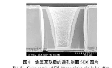
The results show that increasing RF power can greatly improve the etching rate and decrease the sidewall inclination Angle, but the selection ratio decreases, and the sidewall polymer increases accordingly. This is because the increase of RF power leads to the increase of plasma kinetic energy in the chamber, the enhancement of physical bombardment effect, and the etching rate of SiC and mask Ni increases significantly, but the etching rate of mask Ni increases faster. The selection ratio decreased, the inclination Angle decreased, and the sidewall polymer increased. The increase of ICP power can significantly improve the etching rate and the selection ratio, but the side wall inclination Angle becomes steeper and the side wall polymer increases. This is because the increase of ICP power leads to the increase of plasma density in the chamber, the strengthening of chemical action, and the etching SiC rate increases significantly, but it has little effect on the etching mask Ni rate, resulting in the increase of the selection ratio, the increase of the inclination Angle, and the increase of polymer. The influence of the base temperature of the lower electrode has been discussed in detail in the previous article, and will not be repeated here; With the increase of chamber pressure, the sidewall polymer can be reduced, but the etching rate and selection ratio both decrease, which has little effect on the sidewall inclination Angle. This is because with the increase of chamber pressure, the interplasma collision intensifies, the ion mean free path decreases, the ion kinetic energy decreases, the etching SiC and mask Ni rates decrease, but the SiC etching rate decreases faster. As a result, the selection ratio decreased, the sidewall polymer decreased, and the sidewall inclination Angle did not change significantly. With the increase of SF6 flow rate, the sidewall polymer significantly decreases, but the etching rate increases first and then decreases, and the selection ratio also shows a similar change, which has little effect on the sidewall inclination Angle. This is because the plasma density can be effectively increased at the initial stage with the increase of gas flow rate, but the ionization rate becomes worse with the increase of gas flow rate, and the increased gas becomes a diluent gas. The effective etching of SiC can not be achieved, resulting in the etching rate and selection ratio increasing first and then decreasing, but the increased gas can effectively protect the side wall and reduce the side wall polymer, and the change of the side wall inclination Angle is not obvious. By using the new fixture to optimize each process parameter, the etching rate and selection ratio are increased simultaneously, the sidewall polymer is obviously reduced, and the etching inclination Angle is reduced. FIG. 7(a) and (b) are SEM images of through hole etching before and after using the improved fixture, respectively. It can be seen from the comparison pictures that the etching polymer is significantly reduced after using the new fixture and optimizing various process conditions. Finally, the process conditions of etching rate greater than 1μm/min, etching selection ratio greater than 60:1, inclination Angle less than 85° and smooth side wall are obtained. The process conditions are specifically applied to the through-hole profile of a product, as shown in FIG. 8, from which it can also be seen that the through-hole side wall is covered with good metal.
3 Conclusion
Process temperature is an important factor affecting the result of SiC through hole etching. By improving the ICP loading fixture and improving the cooling effect, the wafer surface temperature is reduced during the etching process. After optimizing the process conditions of the equipment, such as RF power, ICP power, lower electrode base temperature and chamber pressure, the SiC through hole process conditions with etching rate greater than 1μm/min, selection ratio of SiC to Ni greater than 60:1, inclination Angle less than 85° and smooth side wall are developed. This technique is suitable for the backside through hole etching of high-power microwave devices such as SiC based GaNHEMT and SiCMESFET and their MMIC development and production, and can shorten the process time and reduce the production cost.
If you are interested in this article, please immediatelycontact us