Please submit your message online, we will contact you as soon as possible!

Author:微组装工艺技术
The so-called ultrasonic welding is the use of ultrasonic frequency vibration energy to weld the same and dissimilar materials method, with the continuous development of technology, ultrasonic welding is widely used in integrated circuits, micromotors, electronic components and other packaging. Ultrasonic welding has the advantages of high efficiency, high speed and automatic, compared with the traditional welding process has become the basic welding process in semiconductor packaging.
First, the basic principle of ultrasonic welding
Ultrasonic energy is essentially a mechanical vibration energy, the operating frequency of 40kHz to 120kHz. The working principle is that the metal material plastic flow under the action of the friction of the metal material, with the temperature rise and high-frequency vibration of the joint area, the atoms in the metal lattice into an active state, and the metal atoms with covalent bonding properties will form an interatomic electron bridge with common electrons within the distance of nanometer units of measurement, and finally form the metal bond.
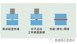
In the process of ultrasonic welding, friction, temperature and molding flow are the three main influencing factors.
Friction is the main heat source and creates a good condition for removing the oxide film on the metal contact surface. The energy required for ultrasonic friction is, is the friction coefficient, is the pressure, is the vibration velocity.
In the actual welding process, the friction coefficient is related to the welding material, the welding head material and the clamping method.
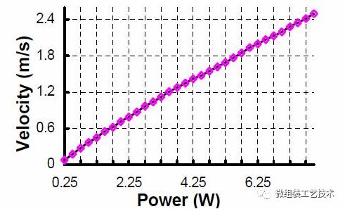
The pressure is related to the fluidity limit of the welded material, the hardness and thickness of the welded material. So there are three basic process variables: amplitude (energy), pressure (force), and time. Because the ultimate goal of the whole process is to divide and disperse the oxide by providing enough energy, these variables are closely related to energy. In addition, in the actual semiconductor packaging manufacturing process, the method of auxiliary heating is often used to promote plastic deformation, and the method of temperature control is relatively simple, and the product is generally placed on the heating clamp platform.
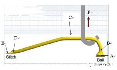
There is also a cold ultrasonic welding process without heating, the welding tool directly acts on the surface of the chip, so the required friction energy is relatively large, and the welded wire is relatively thick. In addition, the main difference between the process and the gold ball pressure welding process in addition to temperature, but also reflected in the welding tool, in general, the gold ball pressure welding tool is mainly ceramic as the base material of the split knife, and cold ultrasonic welding is usually welding aluminum wire, so the welding tool is made of tungsten steel.
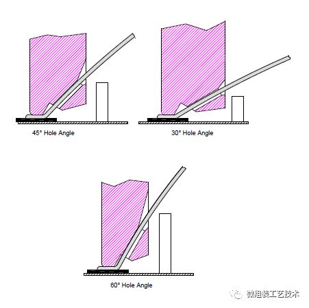
Schematic diagram of wedge welding split cutter head at each Angle
Third, the quality requirements of ultrasonic welding process
The standard to judge whether a solder joint meets the welding quality requirements is often to obtain the strength of the solder joint through destructive experiments, and the usual tensile Test method is called BFrr(Bond Pull Test).
Reference is also sometimes made to the thrust Test, known as the BST(Bond Share Test).
Generally speaking, the greater the welding strength is required, the better, but it is also limited by the strength limit of the material.
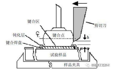
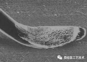
In addition, for the solder joints directly acting on the surface of the chip, in addition to considering the welding strength, it is necessary to check whether the internal structure of the chip is damaged. Generally, the quality index of the research on the welding strength is the tensile force of the welding wire; the method for checking the internal structure of the chip uses saturated strong alkali solution to corrode the solder joints and aluminum layer on the chip surface; This test method is called Etching and observe whether the internal structure is damaged under the microscope with sufficient power.
Fourth, ultrasonic pressure welding process optimization
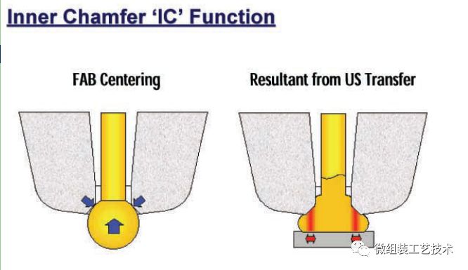
The optimization of ultrasonic pressure welding process is carried out under the premise of the stability of welding equipment and welding materials. If the equipment and welding materials are unstable, the optimization parameters are meaningless, and the results are of no value. Usually we optimize the process by means of experimental design under the premise that all conditions are relatively stable. For example, in the process of playing 50.8um aluminum wire on MOSFET, the difficulty of this process is that the welding area of the gate is limited, and it is very easy to welding off in the way of cold ultrasound. In order to prevent falling off and increase stability, welding parameters need to be increased, but the increase in welding parameters will increase energy and increase the probability of root cracking. To solve this problem, we first determine the general parameter range, this range must ensure the quality of welding, there can be no root cracking phenomenon, and then improve the welding strength as much as possible in this range. In general, if the thickness of the solder joint is more than 25.4um, it can ensure that the root crack can be effectively prevented, which can be calculated and proved by the finite element method in theory.
The general approach to find the parameter range is to select several sensitive parameters according to experience, and do several groups of corresponding experiments to get the corresponding response for fitting analysis. It should be pointed out that the so-called "based on experience" is based on the results of previous tests and exploration. For some new products and new processes, if there is no experience to learn from, it is often necessary to use the method of screen design to screen the main factors and the factors with a large contribution rate. Through mechanical analysis and finite element calculation, it is concluded that the key to reduce stress concentration is to control the thickness of the solder joint and the Angle of the welding line, and to obtain optimization results by studying the motion process and parameter control effect of the equipment. In fact, the optimization of other processes for semiconductor packaging is mostly similar, and the use of optimization methods to stabilize the process can improve the quality and manufacturing level.
| Some of the materials are derived from micro-assembly technology, reprinted only for industry sharing and exchange, does not represent the views of the company, copyright belongs to the original author. In case of infringement, please contact us. In addition, if you reprint this article, please indicate the source.
If you are interested in this article, please immediatelycontact us

Support Hotline
Please submit your message online, we will contact you as soon as possible!