Please submit your message online, we will contact you as soon as possible!

Author:A
Wafer testing is a step performed in the manufacturing process of semiconductor devices. In this step, performed before sending the wafer to the chip for preparation, all individual integrated circuits present on the wafer are tested for functional defects by applying special test modes to them. Wafer testing is performed by a test device called a wafer probe. The wafer test process can be referenced in a variety of ways: wafer Final Test (WFT), electronic Chip classification (EDS), and Circuit probe (CP) are probably the most common.
A wafer probe is a machine used to test integrated circuits (automatic test equipment). For electrical testing, a set of microscopic contacts or probes called probe cards are held in place while the wafers vacuum-mounted on the wafer chuck are moved to the electrical contact state. After one tube core (or array of tubes) has been electrically tested, the probe station moves the chip to the next tube core (or tube core) and the next test can begin. The wafer probe station is typically responsible for loading and unloading the wafer from the vehicle (or box) and is equipped with automatic pattern recognition optics capable of aligning the wafer with sufficient precision to ensure accurate alignment between the contact pad on the wafer and the tip of the probe.
For today's multi-die packages, Examples include stacked chip level packaging (SCSP) or System Level Packaging (SiP) - Developing contactless (RF) probes to identify known test chips (KTDS) and known good chips (KGD) is critical to increasing overall system yield.
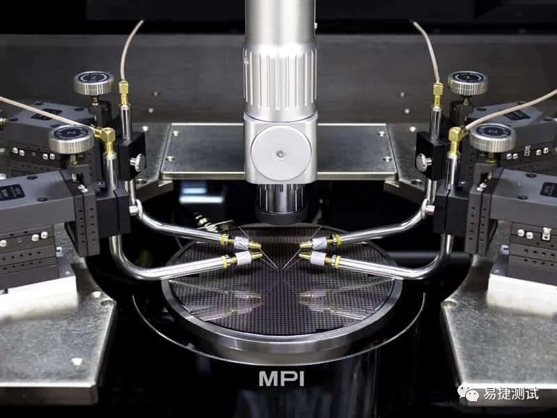
The 8-inch wafer semiconductor Semi-automatic probe station (MPI-TS2000) is in operation
The wafer probe station can also execute any test circuit on the wafer scribing line. Some companies get most of their information about device performance from these scribing test structures.
When all the test patterns for a particular chip pass, its location is remembered for later use in the IC packaging process. Sometimes, the chip has internal backup resources available for repair (i.e., flash ics); If it doesn't pass certain test patterns, these backup resources can be used. If redundancy of the faulty core is not possible, the core is considered faulty and discarded. The fail circuit is usually marked with a small ink dot in the middle of the chip, or the pass/fail information is stored in a file called wafermap. The map classifies passed and failed dies by using bins. Then define bin as a good or bad bare piece. This wafer diagram is then sent to the core connection process, which then picks up the passed circuit by selecting only the bin number of qualified cores. The process of marking a bad chip without ink dots is called substrate mapping. When ink dots are used, the vision system on the subsequent die processing device can disqualify it by recognizing it.
In some very special cases, chips that pass some but not all test modes are still usable as products, often with limited functionality. The most common example is a microprocessor where only a portion of the on-chip cache works. In this case, the processor can sometimes still be sold as a low-cost part with less memory, reducing performance. In addition, when a bad chip (DIE) is identified, the chip in the bad bin can be used by the production staff for line assembly.
The contents of all test modes and the order in which they are applied to the integrated circuit are called test procedures.
After the IC package, the packaged chip is tested again in the IC test phase, and the test mode is usually the same or very similar. For this reason, wafer testing may be considered an unnecessary and redundant step. In practice, this is usually not the case, as removing the defective chip can save the considerable cost of packaging the defective component. However, when the production yield is so high that wafer testing is more expensive than the packaging cost of the defective device, the wafer testing step can be skipped entirely and the bare piece will be blind assembled.
If you are interested in this article, please immediatelycontact us

Support Hotline
Please submit your message online, we will contact you as soon as possible!