Please submit your message online, we will contact you as soon as possible!

Author:Sensing world
MEMS devices utilize semiconductor processing techniques to manufacture three-dimensional mechanical structures, and the three most commonly used MEMS manufacturing techniques include Bulk Micro Machining, Surface Micro Machining, and LIGA.
MEMS refers to microelectromechanical systems, a technology used to make tiny systems composed of electronic and mechanical components. The size of the system may range from a few microns or smaller to a few millimeters. MEMS has proven to be a highly efficient technology with great potential. Some examples of applications for this technology include sensors, accelerometers, printer cartridges, robots, and more.
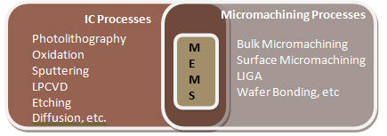
The figure shows the 3 most commonly used MEMS manufacturing techniques
MEMS devices utilize semiconductor processing techniques to manufacture three-dimensional mechanical structures, and the three most commonly used MEMS manufacturing techniques include Bulk Micro Machining, Surface Micro Machining, and LIGA. XJC-S05-T Xinjingcheng Technology 503 series Huba Control WTAL121-N30LM Woosens WSPSS15B20GT Wangsensor Judeshou CS20D sensor advertising
I. Bulk Micro Machining
In bulk micromachining, a large part of the substrate, namely monocrystalline silicon, a very stable mechanical material, is specifically removed to form a three-dimensional MEMS device. A 3D structure diagram of MEMS for bulk micromachining
Bulk micromachining manufacturing of microdevices usually adopts a top-down manufacturing technique, that is, etching on the prepared silicon wafer to produce three-dimensional MEMS components. It is a subtraction process that uses wet anisotropic corrosion or dry etching, such as reactive ion etching (RIE), to create large pits, grooves, and channels. Materials commonly used for wet etching include silicon and quartz, while dry etching is commonly used for silicon, metals, plastics, and ceramics.
Wet etching
In wet etching, the material is removed by dipping it (usually a silicon wafer) into a liquid bath of a chemical etching agent. These etchant can be isotropic (a mixture of HNA - HF, HNO3, and Ch3COOH) or anisotropic (KOH). The anisotropic etchant corrodes faster in the preferred direction. Etching depends on the crystal orientation of the substrate.
Dry etching
In dry etching, high-energy ions accelerate within the plasma phase, providing the material to be etched with the additional energy needed for the reaction. The most common form of MEMS is reactive ion etching (RIE), which uses additional energy in the form of radio frequency (RF) power to drive chemical reactions.
Deep reactive ion etching (DRIE) Deep reactive ion etching (DRIE) is a high aspect ratio etching method that involves alternating high density plasma etching (such as RIE) with protective polymer deposition to obtain a greater aspect ratio.
Piezoresistive effect is a widely used transduction mechanism in volumetric micromechanical sensors such as pressure sensors. In piezoresistive materials, changes in stress cause strain and corresponding resistance changes. Thus, when injected piezoresistive forms at the maximum stress point of the diaphragm (for a pressure sensor), deflection under applied pressure causes a change in resistance.
Second, surface micro-machining
In surface micromachining, three-dimensional structures are constructed by adding and removing a series of thin film layers on the wafer surface in an orderly manner, called structural and sacrificial layers, respectively. Sacrificial layers are deposited and then removed to create mechanical Spaces or gaps between structural layers. The process steps of the surface micromechanical cantilever beam are as follows:
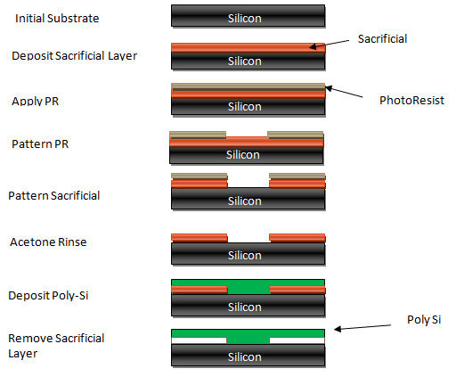
The figure shows the different treatment steps of the surface micromachined cantilever
Many surface micromechanical sensors use capacitance conversion to convert the input mechanical signal into an equivalent electrical signal. In the capacitive conduction method, the sensor can be thought of as a mechanical capacitor in which one plate moves relative to the physical stimulus applied. This changes the gap between the two electrodes and changes the capacitance accordingly. This capacitance change is equivalent to the mechanical stimulation of the input.
LIGA is a German acronym consisting of the letters LI (Roentgen lithography, meaning X-ray lithography), G (galvanizing, meaning electrodeposition), and a (Abformung, meaning molding other materials into a structure with an aspect ratio). Thus, in this technique, a thick photoresist is exposed to X-rays to produce a mold that is subsequently used to form a high-aspect ratio electroplated three-dimensional structure. The LIGA process can produce microparts that are smaller than traditional machining processes and larger than surface micromachined parts. The process steps of LIGA are shown in the figure below.
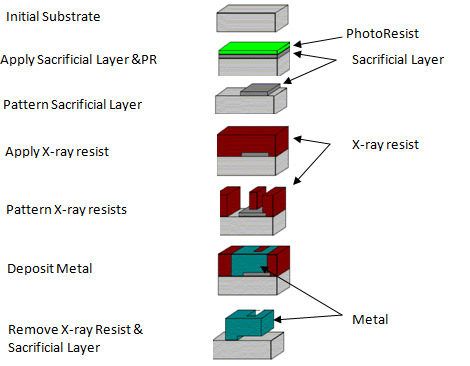
LIGA的处理步骤的图
In order to form complex and large structures, the fusion welding process (using bulk machining and surface micromachining) can be used. It requires atomic bonding of various wafers to create a structure. In this case, the cavity is etched in one piece in the bottom wafer. A second chip is then bonded to form a buried cavity. DRIE mask material is then imprinted on the top wafer. Anisotropic etching is then performed to release the microstructure, and the DRIE masking material is then removed to fabricate the final device.
Disclaimer | Some materials from the sensor world, reprinted only for industry sharing and exchange, does not represent the views of the company, copyright belongs to the original author. In case of infringement, please contact us. In addition, if you reprint this article, please indicate the source.
If you are interested in this article, please immediatelycontact us

Support Hotline
Please submit your message online, we will contact you as soon as possible!