Please submit your message online, we will contact you as soon as possible!

Author:A
To understand the all-around-gate technology, we first have to start with the Field Effect Transistor. The so-called transistor refers to an electronic device equivalent to the role of a faucet. The faucet can be used to control the size and switch of the water flow, similar to the role of the transistor is to control the size and switch of the current. Another key word here is field effect, which means that this control of the current is achieved by applying an electric field. In the transistor structure shown below, we can generate an electric field inside the channel by applying a voltage to the gate. The size of this electric field can be used to adjust the size of the current between the source and the leak. It can also be seen that an important factor determining the efficiency of the FET is the ability of the gate to control the channel.
According to the definition of resistance, we can simply estimate that the size of the resistance between the source and the drain is proportional to the length of the gate. The smaller the gate, the greater the current that can be achieved at the same voltage. This is a key parameter in determining the performance of transistors, which is why early technology nodes were often named according to the length of the gate. The so-called 10 micron node refers to the minimum grid length of 10 microns. Since the introduction of the finned transistor structure, the number in the technical node is merely a marketing code and no longer directly corresponds to any size of the transistor.
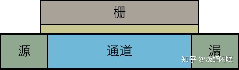
Another important thing to note in the figure above is that the length of the channel is not equal to the length of the gate. This is because the source and drain are achieved by ion implantation. In the process of ion implantation, there will be ions diffused below the gate, forming a so-called diffusion layer. The presence of the diffusion layer makes it impossible to reduce the gate length further after the 32 nm node (avoiding a direct short circuit between the drain and the source). Intel also introduced fin transistors at a later 22nm node.
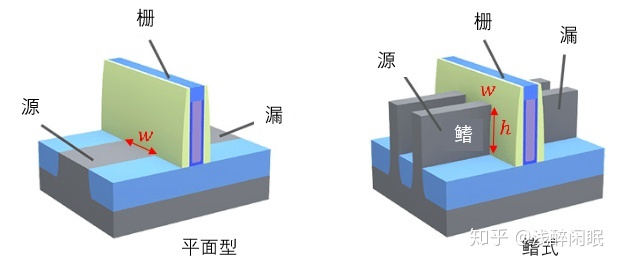
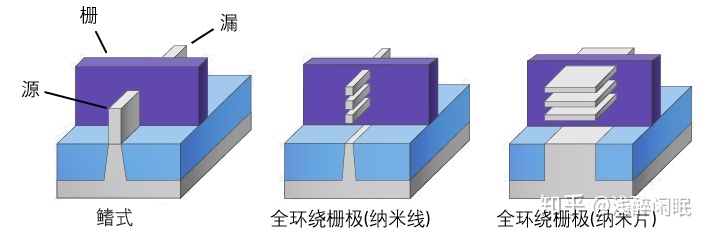
From the planar transistor to the fin transistor, the gate's ability to control the electric field in the channel is greatly improved. The contact area between the gate and the channel was originally determined only by the width of the channel, but in the finned transistor it is determined. The larger contact area results in a larger cross-sectional area for current transmission in the channel, resulting in lower resistance and higher current.
In addition to achieving better control of the channel, another important improvement of the fin transistor is to allow the length of the gate to be further reduced. In planar transistors, the production of source and drain is achieved by ion implantation. In fin transistors, the Source and Drain Epitaxy are grown directly on the fin after the gate is made. At this time, due to the blocking of the gate, there is no diffusion layer, and therefore no problem of short ditch effect.
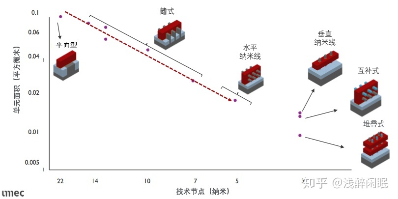
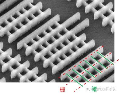
The image below is a scanning electron microscope image given by Intel when the finned transistor was first introduced at the 22nm node. As you can see, each cell contains two sets of fins, three inside each set. In the other direction, the higher line is the grid line. An important parameter to measure the size reduction of Fin transistors is the repetition period of the Fin Line and the Gate Line. The period of the fin line is the smallest of all the structures in the semiconductor device, and the period of the gate line has a decisive effect on the performance of the entire transistor. At the 22 nm node, the fin and grid lines have periods of 60 and 90 nm, respectively. At the 5 nm node, the period of the fin line and grid line is only 27,54 nm.
After 5 nanometers, finned transistors will face a series of problems. First, as the spacing between grid lines decreases further, it is difficult to fill multiple fin lines in a cell as before. If only one fin line is made, the production process is difficult to ensure that the performance of different devices is consistent. Because controlling the average size of multiple fin lines is much easier than controlling the size of a single fin line. The second and more fatal problem is that as the spacing between the gate lines is further reduced, the electrostatic problem of the fin transistor is rapidly increased and directly restricts the further improvement of the transistor performance. The electrostatic problem mentioned here refers to a series of parasitic capacitance and resistance problems caused by the structure of the fin transistor itself. For example, the parasitic capacitance between the gate and the gate, the parasitic capacitance between the gate and the channel, the parasitic capacitance between the gate and the metal electrode, and the parasitic resistance between the source and the drain and other problems. IMEC's previous simulations showed that when the gap between the gate lines shrinks to 40 nanometers, the performance of the fin transistor will become saturated. Therefore, after 5 nm, the industry urgently needed a new structure to replace the fin transistor structure, which led to the all-surround gate transistor.
鳍式晶体管与全环绕栅极的结构对比(图片来源:Samsung)
According to current estimates, a fully encircling gate transistor in the horizontal direction is sufficient to maintain the period of the gate line reduced from 54 nm to about 30~40 nm (2~3 generation nodes). After that, the development of transistors was full of challenges and uncertainties. Among the currently known alternatives, the vertical nanowire structure will adjust the nanowires to a vertical orientation; A complementary architecture would stack N-type and P-type transistors vertically; Stacked structures stack multiple grids in vertical rows. These new structures will theoretically show superior performance over horizontal nanowires/sheets, but they will also require more advanced technology levels to achieve commercial production. From the current information, the complementary structure is the most likely choice after the all-surround gate transistor. But as for what kind of structure it will go to in the future, we will wait and see!
Next generation transistor structure development (image from IMEC)
Disclaimer | Some of the material is from the light drunk idle sleep, reproduced only as an industry sharing exchange, does not represent the views of the company, copyright belongs to the original author. In case of infringement, please contact us. In addition, if you reprint this article, please indicate the source.
If you are interested in this article, please immediatelycontact us

Support Hotline
Please submit your message online, we will contact you as soon as possible!