In the exploration of the development direction of advanced processes below 5nm, the international semiconductor equipment giant Applied Materials AMAT has also carried out a layout in the research of transistor devices, and studied the performance of CFET devices and the selection of MOS tube structures, whose results were published in SISPAD 2020. CFET is a transistor structure that achieves area reduction by stacking nMOS and pMOS in the vertical direction, and well-known research institutions such as IMEC believe that this is an inevitable solution for integrated circuit processes below 3nm.
Research background
With the continuous development of integrated circuit manufacturing technology, due to the bottleneck of electrostatic performance and parasitic parameters in the current silicon-based CMOS process, the road of transistor feature size scaling through FEOL and BEOL processes has come to an end, and CFET (Complementary FET, Complementary field effect transistor (FET) is a new type of transistor structure that can continue the area scaling of integrated circuits.
First, CFET devices realize the stacking of pMOS and nMOS in the vertical direction, which saves the layout space in the horizontal direction. Second, vertical stacking simplifies the terminal access process between pMOS and nMOS. This makes it possible to design a cell library with a smaller number of M0* (critical metal layers) and further reduce the height and area of the standard cells.
Various studies have shown that using CFET architecture can save at least 25% of the area of logic modules and SRAM. In the structural design of CFET devices, both FinFET and nanosheet transistors are the main candidates. For example, IMEC's research results on CFET devices reported in the previous column use CFET devices that stack N-type nanosheet transistors on P-type FinFET.
The research team at AMAT Applied Materials focused on the evaluation and comparison of FBC (FIN-based structure, that is, p/n transistors are FinFET) and SBC (sheet based structure, that is, p/n transistors are nanosheet FET). Relevant results are described in "Complementary FET Device and Circuit Level Evaluation Using Fin-Based and Sheet-Based Configurations Targeting 3nm. "Node and Beyond" was presented at the IEEE International Conference on Semiconductor Process and Device Simulation (IEEE SISPAD). Ashish Pal, El Mehdi Bazizi and other seven researchers of Applied Materials are co-authors of the paper. Liu Jiang is the corresponding author.
*M0: The first layer of metal in the metal post-process, often called the critical metal layer. In fabs, TSMC and Intel define this layer as M0, while Samsung calls it M1.
* Standard Cell library: The most basic type of IP library. In a standard cell library, from system behavior description, logic synthesis, logic function simulation, to timing analysis, verification, and even automatic layout and routing in layout design, there is a rich content and complete function of the cell library support.
Research content
The research team used 3D-TCAD to simulate the CFET process and compare the characteristics of Fin-based and Sheet-based CFET devices. In order to accurately compare the performance of the two structures, the research team constructed a drift diffusion study model and passed the Boltzmann transport equation by quasi-classical * sub-band *. The results show that under the same effective channel width, the nMOS of chip type CFET is 10% higher than that of fin type CFET. For pMOS, the drive current of chip CFET is 5% lower than that of fin CFET. Under the same packaging process standard, the driving current of nMOS and pMOS of chip CFET is 73% and 47% higher than that of fin CFET, respectively, with the increase of nanosheet width as the variable. Taking the 31-stage ring oscillator as a typical circuit model, the performance of chip CFET is 2.6% higher than that of fin CFET when Vdd=0.7V with the same channel width. In the same device area, chip CFET circuit performance is 9% higher than fin CFET.
* Quasi-classical, also known as semi-classical, means that under certain conditions, the electron is approximately treated as a classical particle, and basically reasonable results are obtained. Such models are called quasi-classical models, which are suitable for conditions such as constant weak external fields. The specific treatment methods are as follows: classical treatment of external field, band theory of quantum mechanics treatment of lattice periodic field.
* Boltzmann Transport Equation, an equation proposed by Ludwig Boltzmann to describe the statistical behavior of thermodynamic systems in non-equilibrium states.
The process flow and key parameters of 3nm CFET were simulated
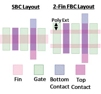
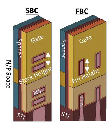
Layout diagram of vane CFET and fin CFET
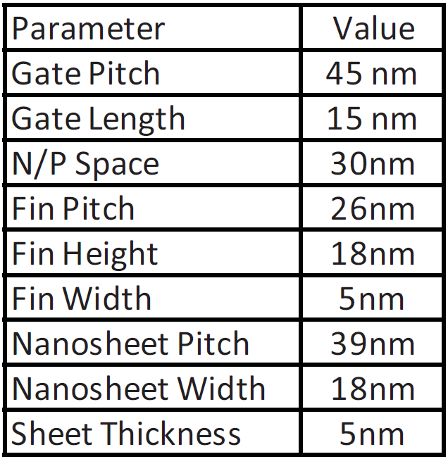
Transistor structure diagram, fin channel width/height of 5nm/18nm,
It can be seen that the chip CFET has a smaller Gate pitch.
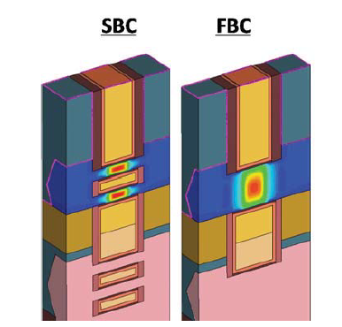
Electron mobility distribution in nMOS
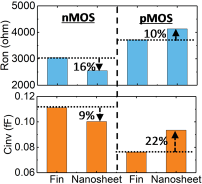
Comparison of on-resistance (Ron) and input capacitance (Cinv)
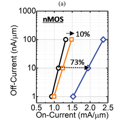
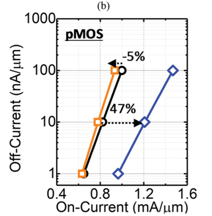
Comparison of Ion-Ioff performance of three CFET structures
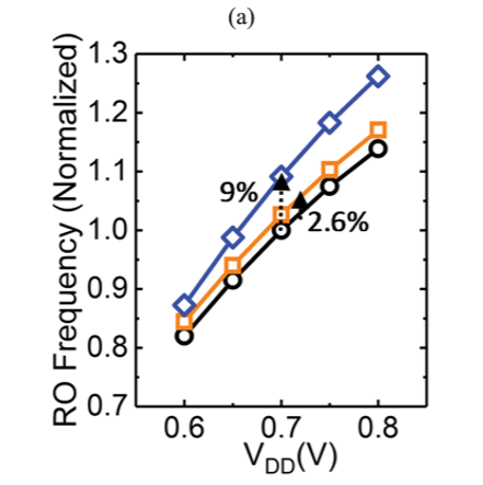
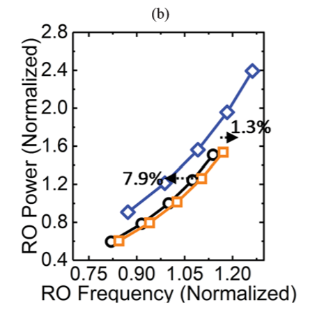
Comparison of the performance of three CFET structure ring oscillators black orange blue corresponding to fin type and groove width 18/31nm wafer base
Prospect
CFET structure is a kind of revolutionary device structure, which is the focus of research in the field of nanotransistor structure. Although the process flow of CFET is very complex, which will also lead to its high production difficulty and cost, its excellent effect in reducing the transistor area is likely to be the solution path of the next generation of CMOS miniaturization processes in the future.
As the "large and complete" representative of the international giant applied materials, not only in the research and development of equipment technology, but also in the frontier research field of advanced device structure, the level of academic research is no less than IMEC and other research-oriented institutions, its technical layout is forward-looking. This is also a microcosm of the characteristics of "strong and constant strength" in the field of integrated circuits, that is, international giants with a monopoly position are able to invest more resources in the field of research and development to obtain greater technological leadership, which is translated into market share.
Disclaimer | Some of the material is from AMAT, reproduced only as an industry sharing exchange, does not represent the views of the company, copyright belongs to the original author. In case of infringement, please contact us. In addition, if you reprint this article, please indicate the source.
If you are interested in this article, please immediatelycontact us