Since the second half of 2020, various mobile phone chip manufacturers have begun a fierce 5nm chip competition, Apple, Huawei, Qualcomm, Samsung have launched the flagship 5nm mobile processor, and claimed that both in performance and power consumption have excellent performance.
However, from the actual performance of these 5nm chips, some users do not buy it, that the performance of 5nm mobile phone chips has not met expectations, and 5nm chips seem to have suffered a collective "rollouts".
5nm chips collectively "flip over", from 7nm to 5nm embarrassment
The earliest commercial 5nm chip is the A14 bionic chip equipped with iPhone12 series mobile phones in October last year, which reaches 11.8 billion transistors, nearly 40% more than A13, and the 6-core CPU and 4-core GPU improve its CPU performance by 40%, graphics performance by 30%, and power consumption by 30%.
Then Huawei released the Kirin 9000, integrated 15.3 billion transistors, 8-core CPU, 24-core GPU and NPU AI processor, the official said that its CPU performance increased by 25%, GPU increased by 50%.
In December, Qualcomm and Samsung have released the Snapdragon 888 and Exynos 1080 manufactured by Samsung, which also claim that performance has been greatly improved and power consumption has been reduced.
The first suspected "rollover" was A14.
According to foreign media 9to5Mac reports, some iPhone 12 users have encountered high power consumption problems when using the phone, standby power dropped by 20% to 40% overnight, whether it is during the day or at night, regardless of whether more background programs are opened, the result is still the same.
The most widely criticized by users is also Snapdragon 888.
In the test of the first users, many digital evaluation bloggers have pointed out that the performance of the Xiaomi 11 of the first Snapdragon 888 has limited improvement, and the power consumption has directly increased. Some people attribute this to the immaturity of the 5nm process of Samsung, the foundry of Snapdragon 888, and Samsung's two 5nm chips are also facing the risk of "rolover" since then.
If according to Moore's Law, the number of transistors in the chip doubles every 18 months, the performance will also double, but the transistor is becoming more and more difficult, and now in the promotion from 7nm to 5nm, the performance of the mobile phone chip seems to be unsatisfactory, not only limited in terms of performance improvement, power consumption is also "flip", facing the embarrassment of advanced process cost performance.
Why do 5nm chips frequently flip over? When the chip process becomes more advanced, how does the performance and power consumption change?
Design performance priority, manufacturing process is not mature
The power consumption of integrated circuits can be divided into dynamic power consumption and static power consumption.
Dynamic power consumption is easy to understand and refers to the power consumption generated when the circuit state changes. The calculation method is similar to that of ordinary circuits. According to the physical formula P=UI, dynamic power consumption is affected by voltage and current.
Static power consumption is the power consumption generated by the leakage current of each MOS tube, although the leakage current generated by each MOS tube is very small, but because a chip is often integrated with hundreds of millions or even tens of billions of transistors, resulting in a large static power consumption of the chip as a whole.
In the chip process development process, when the process is not too advanced, the dynamic power consumption accounts for a large proportion, the industry by giving up the original 5V fixed voltage design mode, the use of isometric buck to slow down the growth rate of power consumption.
However, the voltage reduction also means that the transistor switching will be slower, and some manufacturers who pay more attention to performance will still maintain a 5V supply voltage even if they use more advanced processes, which ultimately leads to increased power consumption.
With the progress of process nodes, the importance of static power consumption has gradually emerged. From the chip process development of Intel and IBM, it can be seen that in the evolution of the process from 180nm to 45nm, the transistor integration growth rate is different, dynamic power consumption or increase or decrease, but static power consumption has been on the rise, and static power consumption is almost the same as dynamic power consumption at 45nm.
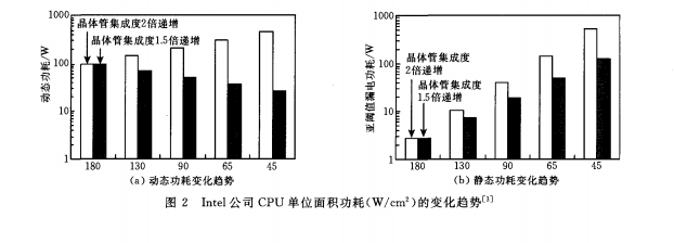
Although some designers are willing to sacrifice power consumption to improve performance, they also have to face the negative impact of high power consumption. For users, serious equipment heating and serious power consumption is the direct impact of high power consumption, if the chip heat dissipation is not good, serious will lead to chip abnormalities or even failure. Therefore, the industry still regards low-power design as one of the problems that the chip industry needs to solve, and how to balance the performance, power consumption and area (PPA) of the chip under the advanced node is also the challenge of chip design and manufacturing. Theoretically speaking, the more advanced the chip process, the lower the power supply voltage produces lower dynamic power consumption, with the further reduction of the process size, the chip voltage that has been reduced to 0.13V is difficult to further decline, so that in recent years, the process size is further reduced, the dynamic power consumption can not be further reduced.
In terms of static power consumption, the channel parasitic resistance of FET decreases with the progress of node, and the power of a single FET decreases with the constant current. On the other hand, the doubling of the number of transistors per unit area increases the static power consumption, so the final static power consumption per unit area may remain unchanged.
Manufacturers in pursuit of lower costs, with a smaller area of the chip to carry more transistors, it seems to be achieved the more advanced the process, the better the chip performance, the lower power consumption. But the actual situation is often much more complicated, in order to improve the overall performance of the chip, some people add the core, some people design more complex circuits, followed by more paths to stimulate power growth, and new methods are needed to balance power consumption.
FinFET, which has a significant impact on the chip industry, is one of the ways to balance chip performance and power consumption. By controlling the connection and disconnection of the circuit through a fish-fin architecture, the circuit control is improved and the leakage current is reduced. The transistor channel is also greatly shortened and the static power consumption is reduced.
However, the evolution from 7nm to 5nm is more complicated.
Oliver King, chief technology officer of Moortec, said in an interview with foreign media: "When we upgrade to 16nm or 14nm, the processor speed has improved a lot, and the leakage current has dropped more quickly, so that we can do more with limited power when using the processor. But when you go from 7nm to 5nm, the leakage becomes very serious again, almost the same as the 28nm level, and now we have to balance them." Kam Kittrell, senior product management director for Cadence's Digital and signage group, said, "A lot of people don't understand what can consume so much power, and they need to get information about the workload in advance to optimize the dynamic power consumption. We've been so focused on static power for so long that once you switch to a FinFET node, dynamic power becomes a big issue. There is also the risk of multiple cores overloading the system, so smarter solutions are needed." This is a common problem faced by 5nm chip design and manufacturing companies, so it is possible to slightly understand why several existing 5nm chips collectively "flip over". Immature design and manufacturing will affect the maximum compromise between performance and power consumption, and of course, it does not rule out the case that chip designers are unwilling to spend great efforts to reduce power consumption in pursuit of better performance chips. Embarrassingly, the top of the process, the greater the need for capital investment, in fact, the pursuit of advanced processes such as 7nm, 5nm and other areas of the field is not much, if the advanced process can not be greatly improved in power consumption and performance, then the pursuit of more advanced process seems to no longer have the original significance.
Going to 3nm, are you really ready?
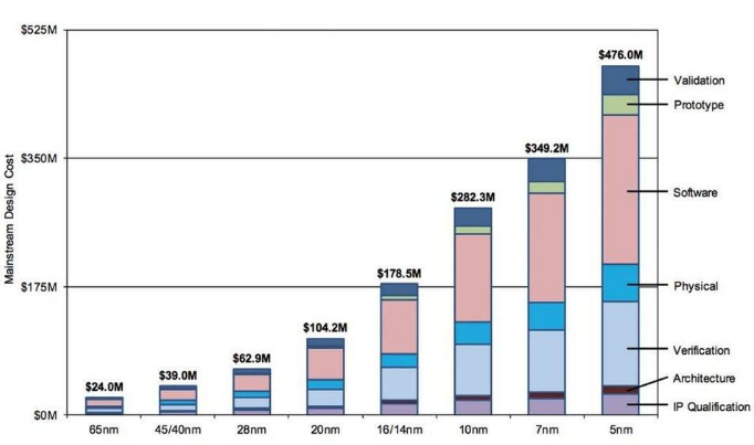
According to the data given by the market research agency International Business Strategies (IBS), the design cost of 65nm process only needs $24 million, to 28nm process needs $629 million, 7nm and 5nm cost has increased rapidly. The 5nm design cost $476 million.
Meanwhile, according to a paper prepared by two authors from the Center for Security and Emerging Technologies (CSET) at Georgetown University's Walsh School of Foreign Service titled "AI Chips: What They Are and Why They Matter "report, the author with the help of a model estimate that TSMC may charge about $17,000 per 5nm wafer, which is nearly twice that of 7nm.
In the estimated model, the authors estimated that each 5nm chip would require $238 in manufacturing costs, $108 in design costs, and $80 in packaging and testing costs. This makes the total cost of each 5nm chip as high as $426 (about 2939 yuan) for the chip design company.
This means that whether it is a chip designer or a chip manufacturer, following Moore's Law to develop to 5nm and below advanced processes, in addition to the need to break the technical bottleneck, but also need to have a huge capital as support, through the research and development cycle and test cycle, to provide the market with improved power consumption and performance of the chip eventually into the return period.
Therefore, not everyone in the industry is positive and optimistic about the advancement of 5nm chips. Amin Shokrollahi, CEO of chip IP supplier Kandou, said in an interview with foreign media: "For us, going from 7nm to 5nm is annoying, the circuit will not scale to scale, and there is a lot of expense, we don't see the advantage of this." But customers want us to do it, so we have to do it."
Global Foundries, the world's second largest chip foundry, announced in 2018 that it would shelve the 7nm project and return resources to 12nm/14nm for economic considerations. Even the powerful Intel has been blocked many times in the development process of 10nm and 7nm.
However, this still does not prevent various mobile phone chip designers from competing in advanced manufacturing processes, and it does not prevent Samsung and TSMC from competing for process supremacy.
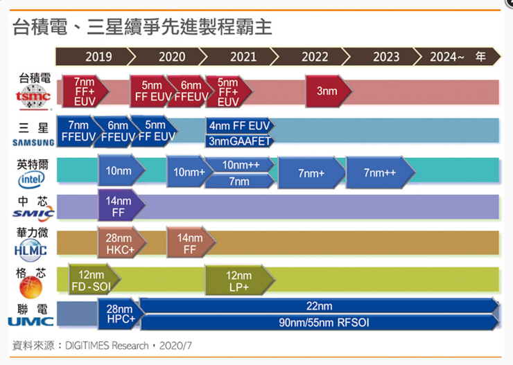
In terms of advanced process chip manufacturing, Samsung regards TSMC as its biggest competitor. In the competition with TSMC, Samsung has promoted advanced process intermittently, and has jumped directly from 7nm to 7nm LPP EUV in order to pre-empt the process, and both will achieve mass production of 5nm FF EUV in 2020. Now they have invested heavily in 3nm research and development and mass production.
TSMC CEO Wei Zhe Jia announced at the investor meeting that TSMC's capital expenditure in 2021 will be as high as $25 billion to $28 billion, of which 80% will be used in advanced processes including 3nm, 5nm and 7nm, 10% will be used in high-end packaging and mask functions, and 10% will be used in special processes.
According to the progress of TSMC's 3nm process, it is expected to trial production in 2021 and enter mass production in the second half of 2022, helping Intel to contract 3nm processor chips.
At the same time, Samsung has also said that the cost of its 3nm GAA may exceed $500 million, and it is expected to use a more advanced GAAFET 3nm process chip than FinFET in mass production in 2022.
Returning to the actual situation of 5nm mobile processors, no matter which manufacturer's design and production, are facing performance and power problems, 5nm chips seem to be immature, 3nm mass production will start trial production this year. Getting closer and closer to the limit of Moore's Law at 3nm, are you really ready?
Reference sources for this article:
https://www.leiphone.com/news/202009/ft8Mx9l2A1T3kCru.html
https://semiengineering.com/power-and-performance-optimization-at-7-5-3nm/
http://www.paper.edu.cn/scholar/showpdf/MUT2EN1IOTD0Mx3h
| Some of the materials are from the Internet, reproduced only as industry sharing and exchange, do not represent the views of the company, copyright belongs to the original author. In case of infringement, please contact us. In addition, if you reprint this article, please indicate the source.
If you are interested in this article, please immediatelycontact us