Please submit your message online, we will contact you as soon as possible!

Author:A
MEMS sensor is the most popular sensor manufacturing technology today, and it is also an important promotion of sensor miniaturization and intelligence, and MEMS technology has promoted the great development of sensors.
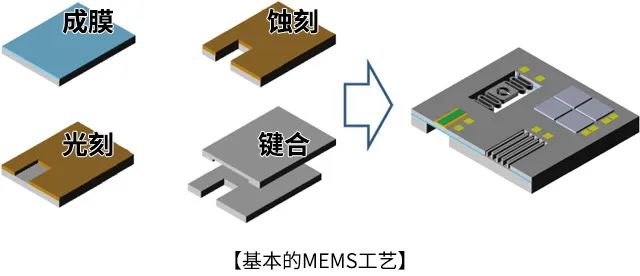
Some key technologies of MEMS process are introduced below.
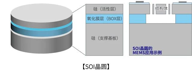
SOI wafer
SOI, short for Silicon On Insulator, refers to a silicon wafer that forms a single crystalline silicon layer on top of an oxide film. It has been widely used in power components and MEMS, where the oxide film layer can be used as the barrier layer for silicon etching, so complex three-dimensional structures can be formed.
TAIKO Grinding "TAIKO" is a trademark of DISCO Corporation
TAIKO grinding is a technology developed by DISCO that keeps the outermost edge of the wafer when grinding, and only grinds its inside.
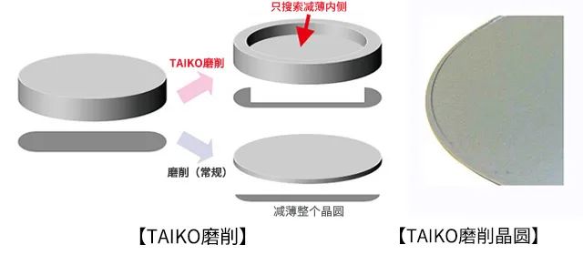
TAIKO grinding has the advantages of "reduced wafer curvature", "higher wafer strength", "easy handling", and "higher integration with other processes" compared to normal grinding.
Wafer bonding/hot strip process
Thin wafers can be easily treated by using support wafers and hot strip wafers.
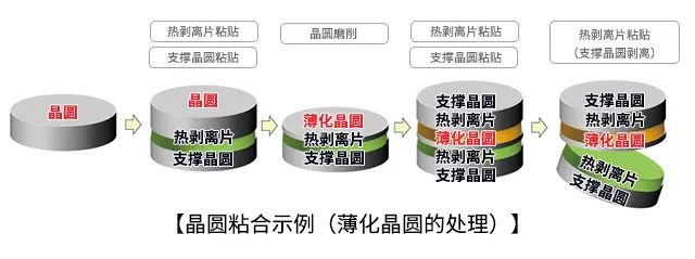
Wafer bonding
Wafer bonding is roughly divided into two categories: "direct bonding" and "bonding through the intermediate layer".
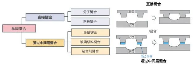
Direct bonding, which does not use adhesives, is a bonding that uses intermolecular forces generated by heat treatment to bond wafers to each other, and is used to make SOI wafers.
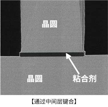
Bonding through an intermediate layer is a bonding method that makes wafers bond to each other by means of adhesives, etc.
Disclaimer: The contents of this article are the author's personal views and do not represent the views or positions of Kaiyi Technology. For more views, please contact us.
If you are interested in this article, please immediatelycontact us

Support Hotline
Please submit your message online, we will contact you as soon as possible!