中文

Advanced process definition

Author:KANA

Advanced process refers to the changes and new systems brought by microelectronics technology, automation technology, information technology and other advanced technologies to the wafer manufacturing technology of the integrated circuit industry. Several of the most advanced process nodes are constantly evolving and upgrading over time. There currently seems to be no standard definition of Advanced process - instead, Advanced Manufacturing Technology (AMT) has a certain term.


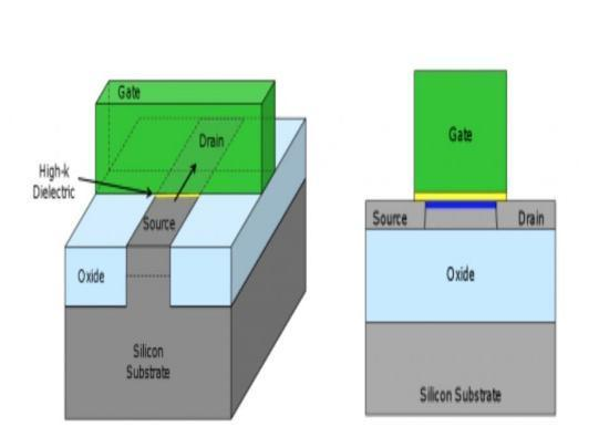
The chip process refers to the spacing between circuits in an integrated circuit, specifically, the line width of the gate in the transistor structure, which is the value in the nanoprocess. The narrower the width, the lower the power consumption.

The main purpose of shrinking the transistor is to cram more transistors into a smaller chip, so that the chip will not become larger due to technological improvements; Secondly, the computing efficiency of the processor can be increased. In addition, reducing the size can also reduce the power consumption; Finally, after the size of the chip is reduced, it is easier to plug into mobile devices (such as mobile phones) to meet the needs of the future thin and light.


The biggest driving force for semiconductor manufacturers to move to smaller process sizes is cost reduction. The smaller the component, the more chips can be cut out of the same wafer. Even if smaller processes require more expensive equipment, their investment costs can be offset by more chips.
The industry takes 28nm as the dividing line between advanced process and mature process, 28nm is between 32nm and 22nm, the industry introduced the high-k value insulation layer/metal gate (HKMG) process at the earlier 45nm stage, and introduced the second-generation high-k insulation layer/metal gate process at 32nm. These laid the foundation for the gradual maturity of 28nm. In the later advanced process, starting from 22nm, FinFET (fin-type field effect transistor) is used. It can be seen that 28nm is just at the key point of the process transition, which is also an important reason for its cost-effective.


When we complete the localization of the 28nm whole industry chain, the global process has taken a step forward, and perhaps 14nm is the dividing line between advanced process and mature process.
Finally, why do some people say that major factories will face serious challenges to enter the 10-nanometer process? The main reason is that an atom is about 0.1 nanometers in size. At 10 nanometers, a line has less than 100 atoms, which is very difficult to make, and as long as there is a defect of an atom, such as atoms falling out or impurities during the production process, it will produce unknown phenomena that affect the yield of the product.


If you are interested in this article, please immediatelycontact us

Support Hotline

0755-8658-2286